Semiconductor remover
A remover and semiconductor technology, applied in the processing of photosensitive materials, etc., can solve the problems of insufficient cleaning ability of photoresist, strong corrosion of semiconductor wafer substrate, low substrate corrosion, etc., and achieve the effect of good application prospect
- Summary
- Abstract
- Description
- Claims
- Application Information
AI Technical Summary
Problems solved by technology
Method used
Image
Examples
Embodiment 1
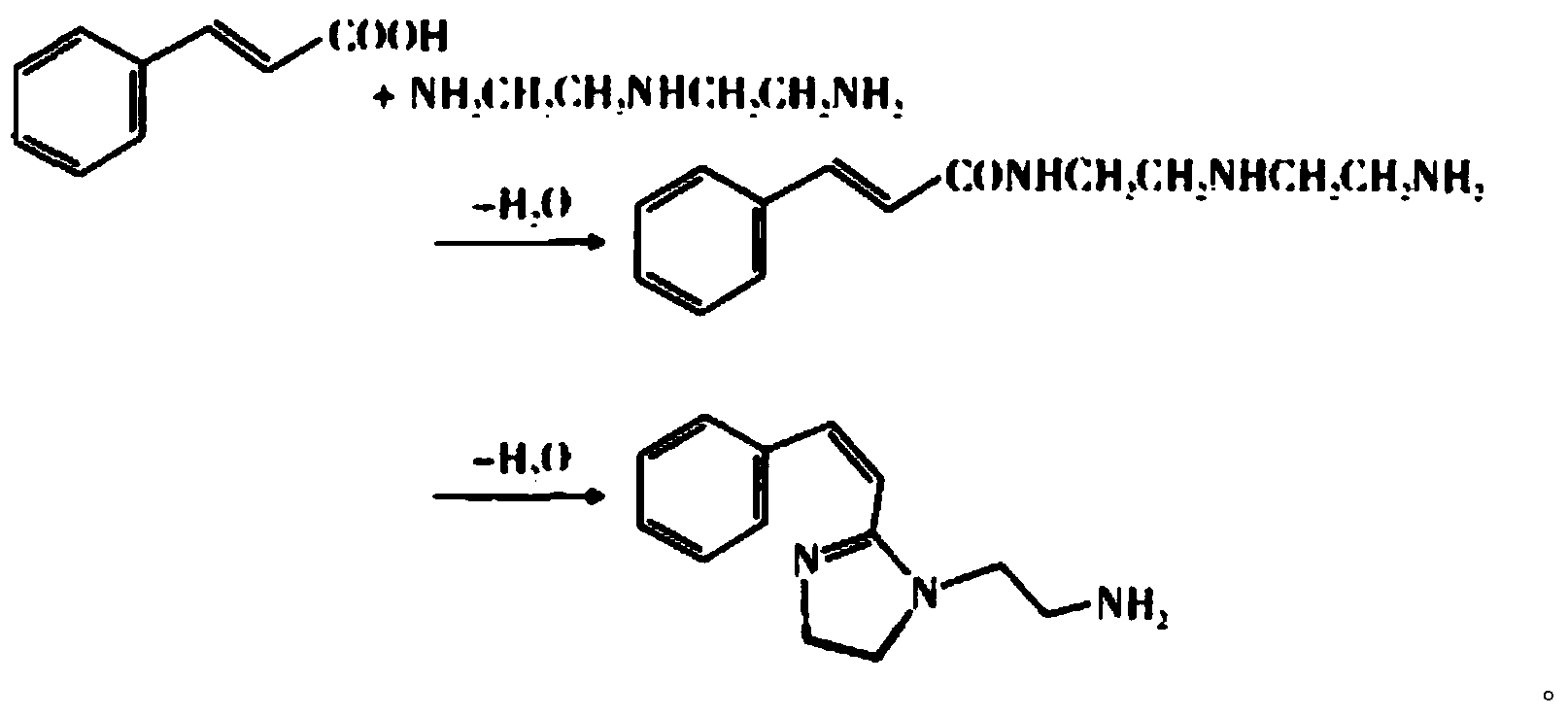
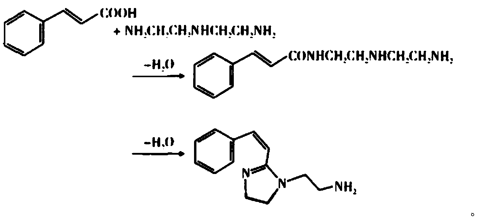
[0044] The preparation of embodiment 1 cinnamyl imidazoline
[0045] Put 10ml of analytically pure diethylenetriamine in a four-necked flask, raise the temperature to 150°C, add 3ml of analytically pure toluene dropwise, add 22g of analytically pure cinnamic acid, stir under nitrogen, and then heat up to 170°C to start acyl After 5 hours of reaction, the temperature was raised to 240° C. to start cyclodehydration for 3 hours. After the reaction was completed, it was placed in a vacuum oven to dry to obtain cinnamyl imidazoline in a brown viscous shape.
Embodiment 21
[0046] Preparation of Example 21,3-bis(2-benzimidazolyl)-2-oxapropane
[0047] Take 10.8g of o-phenylenediamine and 7g of diglycolic acid, mix and dissolve them in 120ml of hydrochloric acid solution with a concentration of 6mol / L, stir mechanically, and reflux at 90°C for 12h. After the system is cooled, adjust the pH with ammonia water value until the solution becomes weakly alkaline, cool, dry, and recrystallize (50mL×3 times) with water-acetone (volume ratio 1:1) to obtain the target product in white powder form, which is 1,3-bis(2-benzene and imidazolyl)-2-oxapropane.
Embodiment 3
[0048] The preparation of embodiment 3 remover 1
[0049] 4g of cinnamyl imidazoline prepared in Example 1, 6g of 1,3-bis(2-benzimidazolyl)-2-oxapropane prepared in Example 2, 40g of N-methylpyrrolidone, 10g of tetramethylammonium hydroxide , 30g of citric acid / ammonium citrate buffered aqueous solution (the mass content ratio of citric acid and ammonium citrate is 10:1), 10g of propylene glycol monophenyl ether were mixed, stirred evenly, and the remover 1 was obtained.
[0050] Comparative Example Comparative Remover
[0051] Mix 40g N-methylpyrrolidone, 10g tetramethylammonium hydroxide, 30g citric acid / ammonium citrate buffer solution (the mass content ratio of citric acid and ammonium citrate is 10:1), 10g propylene glycol monophenyl ether, stir well , that is, compare the remover.
PUM
 Abstract
Description
Claims
Application Information
 - R&D Engineer
- R&D Manager
- IP Professional
- Industry Leading Data Capabilities
- Powerful AI technology
- Patent DNA Extraction
Browse by: Latest US Patents, China's latest patents, Technical Efficacy Thesaurus, Application Domain, Technology Topic, Popular Technical Reports.
© 2024 PatSnap. All rights reserved.Legal|Privacy policy|Modern Slavery Act Transparency Statement|Sitemap|About US| Contact US: help@patsnap.com


