Light-emitting diode packaging structure
A technology of light-emitting diodes and packaging structures, which is applied to electrical components, electrical solid-state devices, circuits, etc., and can solve problems such as cost increase
- Summary
- Abstract
- Description
- Claims
- Application Information
AI Technical Summary
Problems solved by technology
Method used
Image

Examples
Embodiment Construction
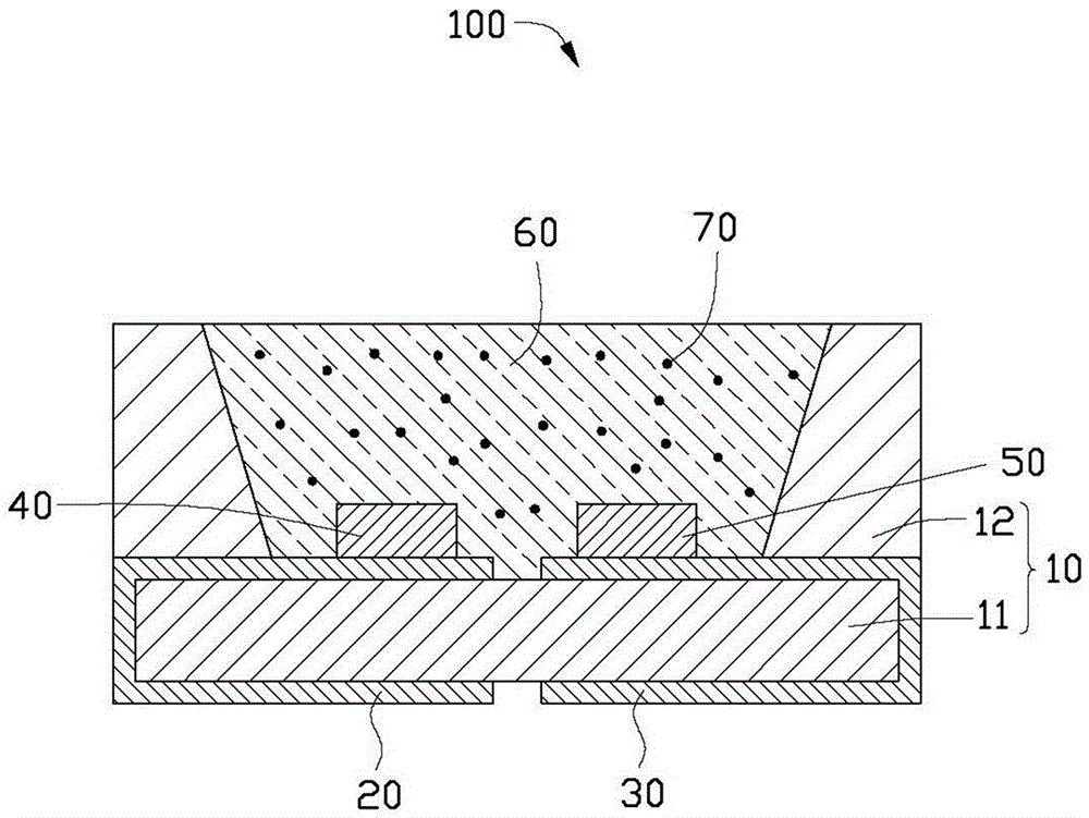
[0009] Please refer to figure 1 , is a schematic cross-sectional view of the light emitting diode package structure 100 provided by the embodiment of the present invention. The light emitting diode packaging structure device 100 includes a base 10, a first lead 20 and a second lead 30 respectively fixed on opposite ends of the base 10, a first lead 20 and a second lead 30 respectively installed on the first lead 20 and the second lead 30. The light emitting diode 40 , the second light emitting diode 50 , and the packaging body 60 covering the first light emitting diode 40 and the second light emitting diode 50 .
[0010] The base 10 includes a base 11 and a reflection cup 12 formed on the base 11 . The reflecting cup 12 is annular, and a recess (not shown) is formed in its middle. Both the first pin 20 and the second pin 30 are made of metal material, bent into a U-shape, and respectively passed through opposite ends of the base 11 of the base 10 . The first pin 20 and the ...
PUM
 Abstract
Description
Claims
Application Information
 - R&D
- Intellectual Property
- Life Sciences
- Materials
- Tech Scout
- Unparalleled Data Quality
- Higher Quality Content
- 60% Fewer Hallucinations
Browse by: Latest US Patents, China's latest patents, Technical Efficacy Thesaurus, Application Domain, Technology Topic, Popular Technical Reports.
© 2025 PatSnap. All rights reserved.Legal|Privacy policy|Modern Slavery Act Transparency Statement|Sitemap|About US| Contact US: help@patsnap.com