SDRAM high-capacity image data register based on FPGA

An image data and buffer technology, applied in the field of data read and write controllers, can solve the problems of complex SDRAM read and write interfaces, unfavorable module migration, unfavorable operations, etc., and achieves the effects of low resource consumption, high timing performance, and easy migration.

Inactive Publication Date: 2014-02-26
UNIV OF ELECTRONIC SCI & TECH OF CHINA
View PDF1 Cites 2 Cited by
  • Summary
  • Abstract
  • Description
  • Claims
  • Application Information

AI Technical Summary

Problems solved by technology

[0005] 2. The interface is complex, the read-write interface of SDRAM is complicated, and there are many signals, w

Method used


Image

  • SDRAM high-capacity image data register based on FPGA
  • SDRAM high-capacity image data register based on FPGA

Examples


Example Embodiment

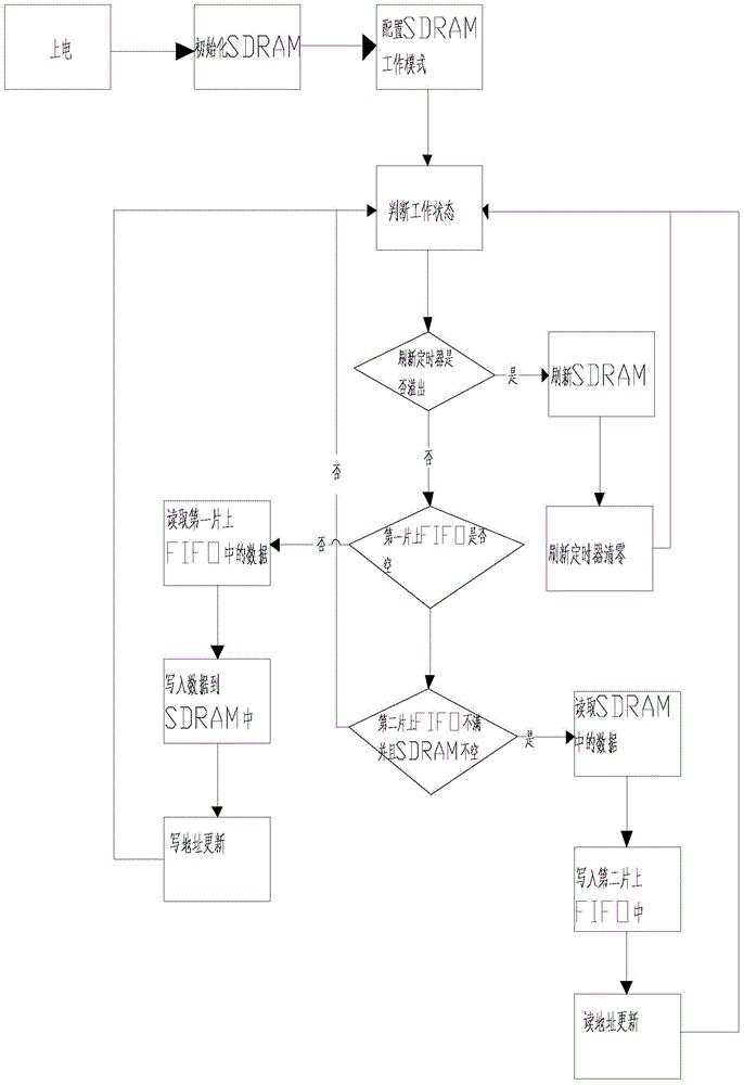
[0020] The present invention will be further elaborated below in conjunction with the accompanying drawings.

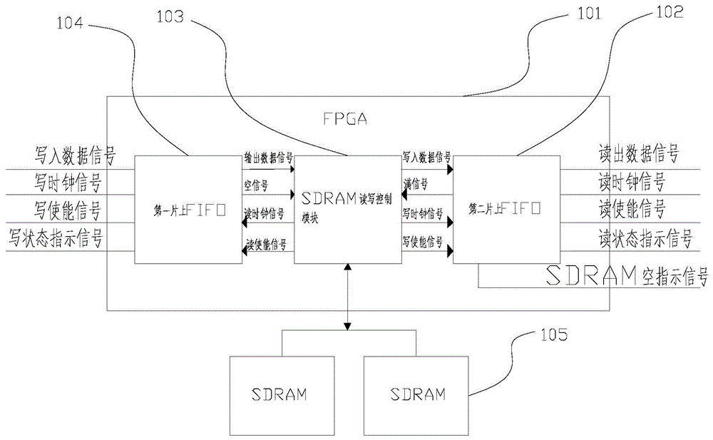
[0021] like figure 1 and figure 2 Shown, a kind of SDRAM large-capacity image data register based on FPGA, comprise FPGA101 and at least two SDRAM105 that are arranged on the outside of FPGA, described FPGA101 is connected with described SDRAM105, it is characterized in that: described FPGA101 includes for the first A first on-chip FIFO104 connected to the signal of the image data buffer write port, a second on-chip FIFO102 and SDRAM read-write controller 103 for connecting the second signal to the signal of the image data buffer read port, said The SDRAM read-write controller 103 is respectively connected to the first on-chip FIFO 104 and the second on-chip FIFO 102 .

[0022] According to an embodiment of the present invention, the first signal includes the input data signal of the first on-chip FIFO104, the write clock signal of the first on-chip FIFO104, the wr...


PUM


Abstract

The invention discloses an SDRAM high-capacity image data register based on an FPGA. The SDRAM high-capacity image data register comprises the FPGA and at least two SDRAMs arranged on the outer portion of the FPGA, and the FPGA is connected with the SDRAMs. The SDRAM high-capacity image data register is characterized in that the FPGA comprises a first on-chip FIFO register, a second on-chip FIFO register and an SDRAM read-write controller, the first on-chip FIFO register is used for connecting a first signal with the signal of an image data register writing port, the second on-chip FIFO register is used for connecting a second signal with the signal of an image data register read port, and the SDRAM read-write controller is respectively connected with the first on-chip FIFO register and the second on-chip FIFO register. The SDRAM high-capacity image data register has the advantages that a complex bus is not needed for control, redundant functions are eliminated, consumed resources are few, timing sequence performance is high, a port is simple, the addresses of the SDRAMs are hidden from the outside, the port facing the outside is like an FIFO register, the operation is simple, and transplantation is convenient.

Description

technical field [0001] The invention relates to a data read-write controller, in particular to an FPGA-based SDRAM large-capacity image data buffer. Background technique [0002] The linear array CIS scanner has the characteristics of simple structure, no additional optical lens, and low cost. It has been widely used in linear array scanning and visual systems of planar products such as plates, paper, and printing. On the scanner, since the image data rate generated by the CIS sensor through AD is often faster than the image processing and transmission rate at the back end, a large-capacity storage device is required to store data. [0003] Existing FPGA-based SDRAM controllers have the following disadvantages: [0004] 1. Using the SDRAM control core made by FPGA manufacturers takes up more resources, resulting in waste of cost and affecting system performance. [0005] 2. The interface is complex, the read-write interface of SDRAM is complicated, and there are many signa...

Claims


Application Information

Patent Timeline
IPC IPC(8): H04N1/21
Inventor 刘霖谭沛岩刘娟秀杨先明张静谢煜任程辉邹修功王耀杰付大鹏孙榕泽刘永
Owner UNIV OF ELECTRONIC SCI & TECH OF CHINA
Why Eureka
Try Eureka