Supercharge Your Innovation With Domain-Expert AI Agents!

Method for preparing antireflection film by plasma enhanced chemical vapor deposition

A technology of anti-reflection coating and plasma gas, which is applied in the direction of gaseous chemical plating, electrical components, semiconductor devices, etc., can solve problems such as instability and changes in photoelectric conversion efficiency of solar cells, and achieve the effect of concentrated conversion efficiency of batteries

Active Publication Date: 2016-01-20
正泰新能科技股份有限公司
View PDF6 Cites 0 Cited by
  • Summary
  • Abstract
  • Description
  • Claims
  • Application Information

AI Technical Summary

Problems solved by technology

Furthermore, due to the change of the deposited thickness of the anti-reflection film, the photoelectric conversion efficiency of the solar cell will change, which is not stable enough.

Method used


Image

  • Method for preparing antireflection film by plasma enhanced chemical vapor deposition
  • Method for preparing antireflection film by plasma enhanced chemical vapor deposition
  • Method for preparing antireflection film by plasma enhanced chemical vapor deposition

Examples


Embodiment Construction

[0042] The following disclosure provides many different embodiments or examples for implementing different structures of the present invention. To simplify the disclosure of the present invention, components and arrangements of specific examples are described below. Furthermore, the present invention may repeat reference numerals and / or letters in different instances. This repetition is for the purpose of simplicity and clarity and does not in itself indicate a relationship between the various embodiments and / or arrangements discussed. It should be noted that components illustrated in the figures are not necessarily drawn to scale. Descriptions of well-known components and processing techniques and processes are omitted herein to avoid unnecessarily limiting the present invention.

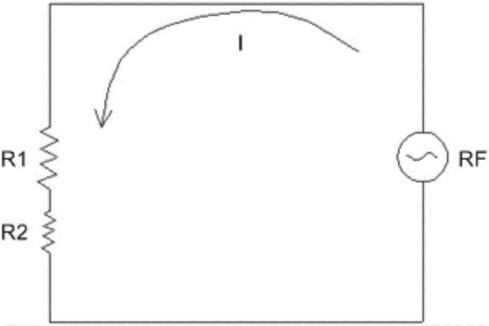
[0043] refer to image 3 , image 3 It is a schematic flowchart of a specific embodiment of a method for preparing an anti-reflection film by plasma vapor deposition according to the present in...


PUM

PropertyMeasurementUnit
thicknessaaaaaaaaaa

Abstract

The invention discloses a method for making an antireflection film by using plasma enhanced chemical vapor deposition, which comprises the following steps: a silicon chip is placed on a support plate, the support plate is placed in a reaction chamber; reaction gas is introduced in the reaction chamber; excitation is carried out through plasma source, the antireflection film is formed on the surface of the silicon chip; the above steps can be carried out for many times in an usage period of the support plate, and the time for plasma source excitation to form the antireflection film can be changed with the usage frequency of the support plate. By using the method of the invention, the time for antireflection film deposition can be correspondingly adjusted with the usage frequency of the support plate, so that the thickness of the antireflection film obtained in the usage period of the support plate is more uniform.

Description

technical field [0001] The invention relates to the field of solar cell manufacturing, in particular to a method for preparing an anti-reflection film by plasma-enhanced chemical vapor deposition. Background technique [0002] Plasma Enhanced Chemical Vapor Deposition (PECVD) uses microwave or radio frequency to ionize the gas containing the constituent atoms of the film to form plasma locally, and the plasma is chemically active and easy to react, and then deposited on the substrate. The method of depositing the desired thin film. Because the anti-reflection film deposited on the surface of silicon wafers by PECVD technology has the advantages of uniform film deposition, good insulation and passivation effect, and fast process speed, PECVD technology is currently widely used in the manufacturing process of crystalline silicon solar energy industry. [0003] refer to Figure 1(a) and Figure 2(a) , in the specific operation process, the carrier plate carrying the silicon w...

Claims


Application Information

Patent Timeline
Patent Type & Authority Patents(China)
IPC IPC(8): C23C16/44H01L31/18
CPCY02P70/50
Inventor 李云峰韩玮智牛新伟仇展炜
Owner 正泰新能科技股份有限公司
Features
  • R&D
  • Intellectual Property
  • Life Sciences
  • Materials
  • Tech Scout
  • Unparalleled Data Quality
  • Higher Quality Content
  • 60% Fewer Hallucinations
Learn More