Deep UV (Ultraviolet) LED and preparation method thereof

A light-emitting diode, deep ultraviolet technology, applied in electrical components, circuits, semiconductor devices, etc., can solve problems such as quantum well absorption loss, and achieve the effect of improving light extraction efficiency and external quantum efficiency.

Inactive Publication Date: 2014-03-26
武汉优炜芯科技有限公司
View PDF6 Cites 15 Cited by
  • Summary
  • Abstract
  • Description
  • Claims
  • Application Information

AI Technical Summary

Problems solved by technology

Although the flip chip process can successfully emit ultraviolet light from the surface of the substrate, at least half of the lumine

Method used


Image

  • Deep UV (Ultraviolet) LED and preparation method thereof

Examples


Embodiment 1

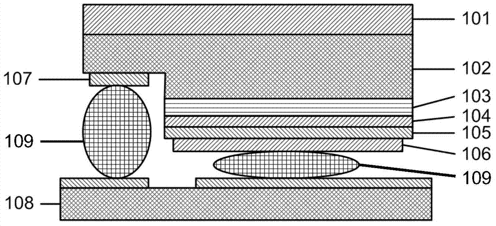
[0032] Such as figure 1 As shown, this embodiment provides a deep ultraviolet light emitting diode, including: a substrate 101, a first n-type AlGaN layer 102 formed on the substrate 101, and a first n-type AlGaN layer 102 formed on the first surface of the first n-type AlGaN layer AlGaN / AlGaN multi-quantum well layer 103, a p-type AlGaN electron blocking layer 104 formed on the AlGaN / AlGaN multi-quantum well layer 103, a second n-type AlGaN layer 105 formed on the p-type AlGaN electron blocking layer 104, formed on The p-type terminal electrode 106 on the second n-type AlGaN layer 105, the n-type electrode 107 formed on the second surface of the first n-type AlGaN layer 102, and the p-type terminal electrode 106 and the n-type electrode 107 respectively through solder 109 soldered flip-chip substrate 108 . Wherein, the second n-type AlGaN layer 105 and the p-type AlGaN electron blocking layer 104 form a tunnel junction, and when the light-emitting diode is in a forward-biase...

Embodiment 2

[0037] This embodiment provides a method for preparing a deep ultraviolet light-emitting diode, which specifically includes the following steps:

[0038] (1) On the substrate, grow the first n-type AlGaN layer;

[0039] Specifically, on the sapphire substrate, using the MOCVD process, the growth temperature was kept at 1150°C, and the Si doping concentration with a thickness of 2000nm was grown at 1×10 20 cm -3 Al 0.6 Ga 0.4 N layers.

[0040] (2) On the first n-type AlGaN layer, grow an AlGaN / AlGaN multiple quantum well layer;

[0041] Specifically, in Al 0.6 Ga 0.4 On the N layer, the growth temperature is kept at 1150°C, and Al 0.6 Ga 0.4 N / Al 0.4 Ga 0.6 N MQW layer, Al 0.6 Ga 0.4 N barrier layer thickness is 10nm, Al 0.4 Ga 0.6 The thickness of the N well layer is 3nm, and the period of the quantum well is 10.

[0042] (3) On the AlGaN / AlGaN multiple quantum well layer, grow a p-type AlGaN electron blocking layer;

[0043] Specifically, the growth temperatu...


PUM

PropertyMeasurementUnit
Thicknessaaaaaaaaaa
Thicknessaaaaaaaaaa
Thicknessaaaaaaaaaa

Abstract

The invention discloses a deep UV LED and a preparation method thereof. The LED comprises a substrate, a first n type AlGaN layer, a AlGaN/AlGaN multi-quantum well layer, a p type AlGaN electron barrier layer, a second n type AlGaN layer, a p type termination electrode, an n type electrode and an inverted substrate, wherein the first n type AlGaN layer includes a first surface and a second surface, the AlGaN/AlGaN multi-quantum well layer is formed at the first surface, and the n type electrode is formed at the second surface; the p type termination electrode is formed at the second n type AlGaN layer; and the inverted substrate is welded with the p type termination electrode and the n type electrode via solders. The LED is formed by tunnel junction at the surface of a device, and the p type termination electrode is made of a metal material which can form good ohmic contact with the n type material and is high in reflectivity, so that the light extraction efficiency of the UV LED is improved, and the external quantum efficiency of the whole device is improved.

Description

technical field [0001] The invention relates to the technical field of semiconductor devices, in particular to a deep ultraviolet light-emitting diode and a preparation method thereof. Background technique [0002] The traditional ultraviolet light sources currently used are gas lasers and mercury lamps, which have disadvantages such as low efficiency, large volume, environmental protection and high voltage. In contrast, the ultraviolet light-emitting diode based on AlGaN semiconductor material is a solid-state ultraviolet light source, which has many advantages such as no mercury pollution, adjustable wavelength, small size, good integration, low energy consumption, and long life. Medical and health fields such as cancer detection and skin disease treatment, rapid decomposition of pollutants such as dioxins, polychlorinated biphenyls, and pesticides, and environmental protection fields such as water and air purification, and high-color-rendering index white light lighting e...

Claims


Application Information

Patent Timeline
IPC IPC(8): H01L33/14H01L33/36H01L33/00
CPCH01L33/145H01L33/0075H01L33/06H01L33/32H01L33/405
Inventor 吴志浩方妍妍戴江南陈长清
Owner 武汉优炜芯科技有限公司
Why Eureka
Try Eureka