System and method for designing FPGA (field programmable gate array) structure
A structure design and structure diagram technology, applied in the field of microelectronics, can solve the problems of error-prone editing of FPGA structure description files, insufficient design flexibility, and inability to adjust FPGA local structures, etc., to improve flexibility, reduce complexity, and quickly and easily performance effect
- Summary
- Abstract
- Description
- Claims
- Application Information
AI Technical Summary
Problems solved by technology
Method used
Image

Examples
Example Embodiment
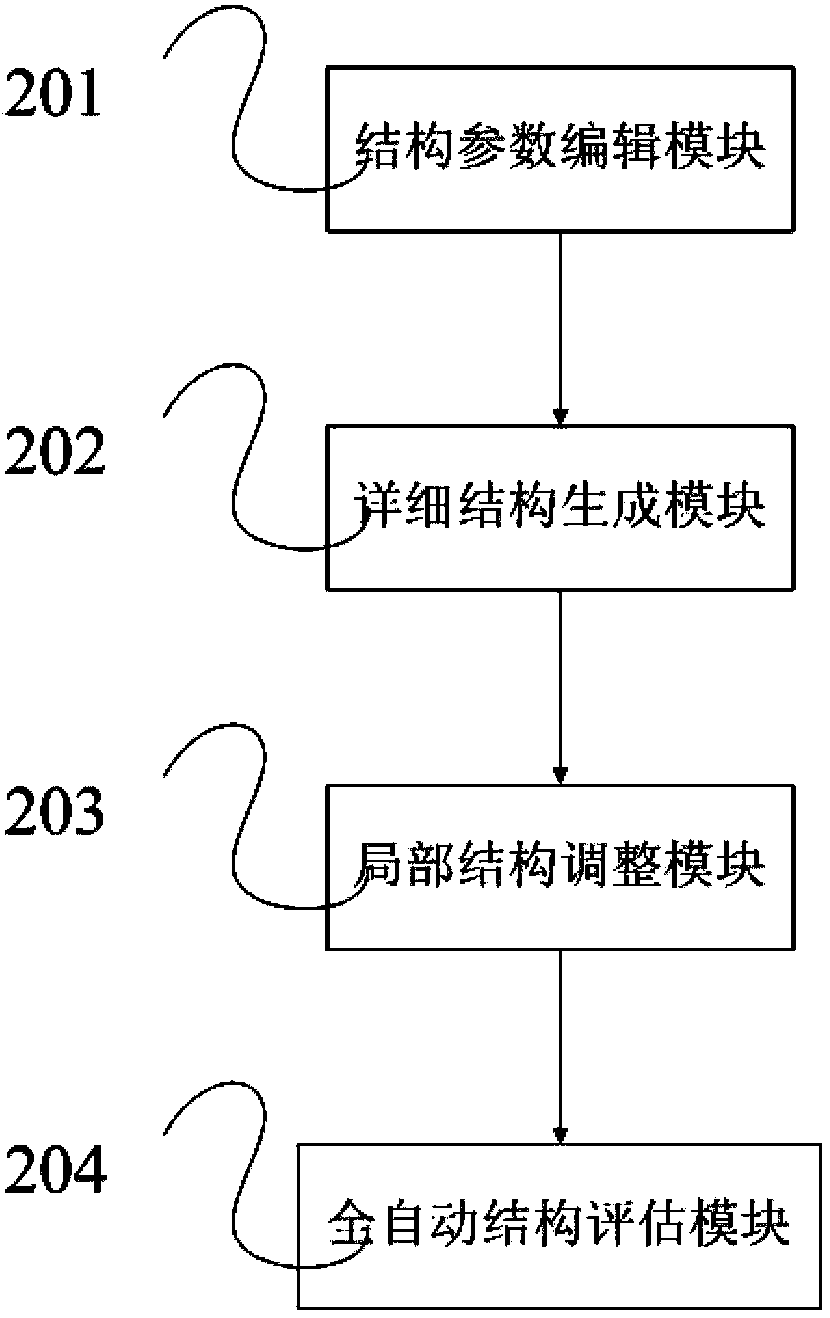
[0034] See figure 1 , A system for FPGA structure design provided by an embodiment of the present invention includes a structure parameter editing module, a detailed structure generation module, a local structure adjustment module, and a fully automatic structure evaluation module;
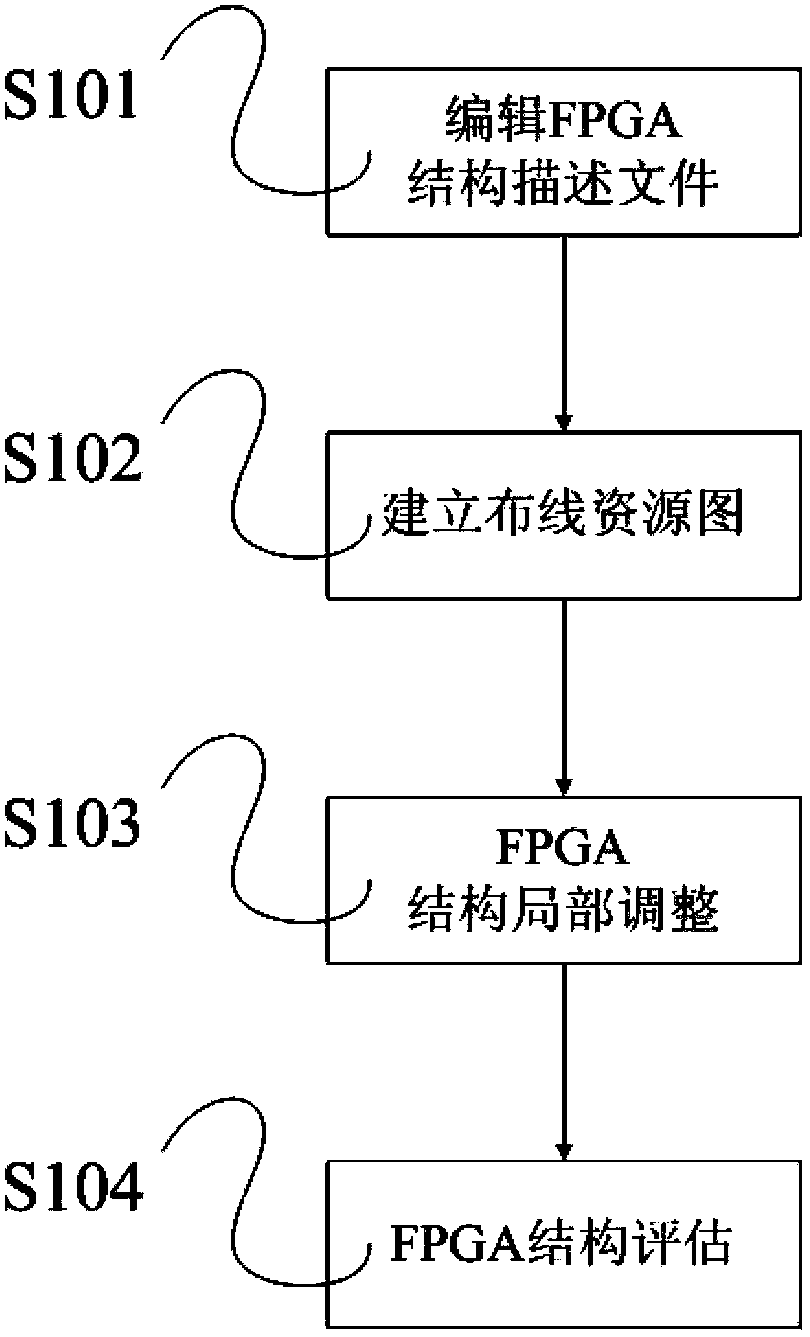
[0035] Among them, the structural parameter editing module is used to select the structural item to be edited, and then set the FPGA structural parameters to generate a structural description file;
[0036] The detailed structure generation module reads the FPGA structure parameters according to the structure project, then builds the wiring resource diagram, and generates the FPGA detailed structure diagram according to the wiring resource diagram;
[0037] The local structure adjustment module partially adjusts the detailed FPGA structure diagram, and then establishes the wiring resource diagram, and generates the FPGA detailed structure diagram according to the wiring resource diagram;
[0038] The fully...
PUM
 Abstract
Description
Claims
Application Information
 - R&D Engineer
- R&D Manager
- IP Professional
- Industry Leading Data Capabilities
- Powerful AI technology
- Patent DNA Extraction
Browse by: Latest US Patents, China's latest patents, Technical Efficacy Thesaurus, Application Domain, Technology Topic.
© 2024 PatSnap. All rights reserved.Legal|Privacy policy|Modern Slavery Act Transparency Statement|Sitemap