Packaging module, packaging terminal and manufacturing method thereof
A manufacturing method and terminal technology, applied in contact manufacturing, semiconductor/solid-state device manufacturing, electrical components, etc., can solve problems such as poor reliability and different stress relief effects, and achieve the effect of improving connection reliability.
- Summary
- Abstract
- Description
- Claims
- Application Information
AI Technical Summary
Problems solved by technology
Method used
Image

Examples
no. 1 example
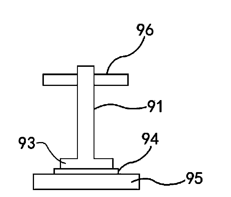
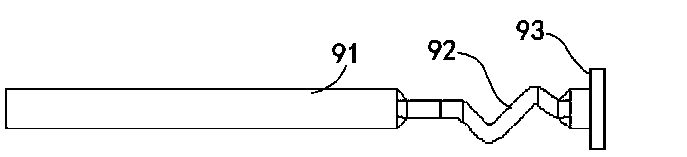
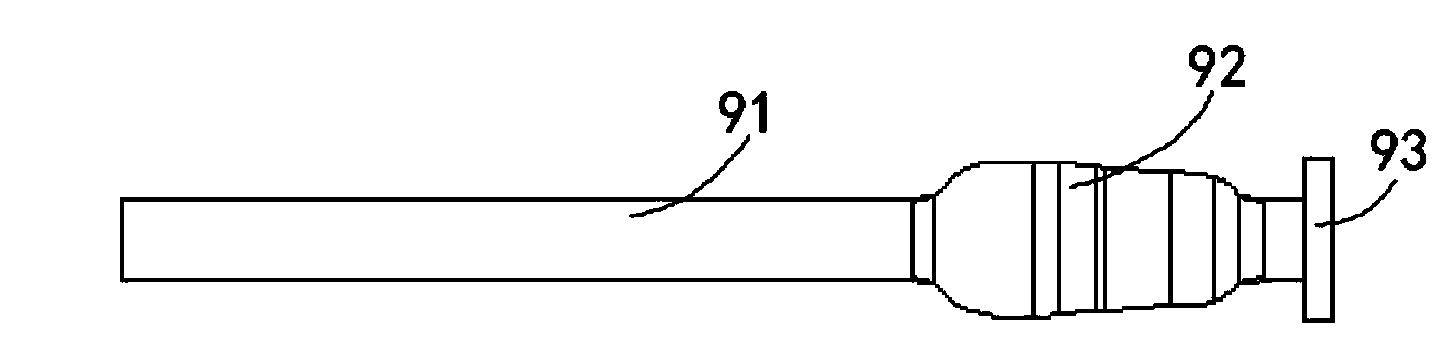
[0051] Such as Figure 5 and Figure 6 As shown, the packaging terminal of the first embodiment of the present invention includes an end part 1, a bent part 2 and a base 3, wherein the first end of the bent part 2 is connected to the end part 1, and the second end of the bent part 2 Connect to base 3. In this embodiment, the end part 1 and the base 3 can be the same as the packaging terminal of the prior art, the difference is that the bent part has a C-shaped bend, and its cross-section is gradual, and the cross-sections of the two ends of the bent part 2 The area is the largest, and the area of the section at the center is the smallest, hereinafter referred to as the second section. The area of the cross-section of the bent part 2 gradually decreases from both ends of the bent part 2 toward the center, and the second cross-section (minimum cross-section) is at the center of the bent part 2, that is, Figure 5 The center position of the C-shaped bend in the left-right ...
no. 2 example
[0075] Figure 13 It is the packaging terminal of the second embodiment of the present invention. The difference from the first embodiment is that a chamfer 10 is added to the top of the end portion 1 . Because the package terminal 12 is positioned through the positioning hole on the PCB circuit board when the package terminal 12 is assembled with the PCB circuit board, in order to improve the assembly efficiency, the positioning hole of the PCB circuit board can be designed with a positive angle. Therefore, the end of the package terminal of this embodiment 1 The top end is chamfered to improve the convenience of assembly.
[0076] In each of the following embodiments, the top of the end portion 1 may be provided with a chamfer 10 , which will not be repeated here.
no. 3 example
[0078] Figure 14A and Figure 14B It is the packaging terminal of the third embodiment of the present invention.
[0079] The difference from the first embodiment is that the cylindrical surface of the base 3 is designed with an inner groove with a depth h. Because the package terminals 12 and the pads of the substrate 11 are soldered by solder, the groove structure on the base 3 can improve the soldering strength.
[0080] There is no essential difference between this embodiment and the first embodiment on the principle of elasticity.
PUM
 Abstract
Description
Claims
Application Information
 - R&D
- Intellectual Property
- Life Sciences
- Materials
- Tech Scout
- Unparalleled Data Quality
- Higher Quality Content
- 60% Fewer Hallucinations
Browse by: Latest US Patents, China's latest patents, Technical Efficacy Thesaurus, Application Domain, Technology Topic, Popular Technical Reports.
© 2025 PatSnap. All rights reserved.Legal|Privacy policy|Modern Slavery Act Transparency Statement|Sitemap|About US| Contact US: help@patsnap.com