Transparent printed circuit board and manufacturing method thereof

A technology for printed circuit boards and production methods, which is applied in the directions of printed circuit manufacturing, printed circuits, printed circuit components, etc., can solve the problems of reducing the transparency of transparent circuit boards, and achieve the effect of enhanced transparency.

Inactive Publication Date: 2014-06-04
AVARY HLDG (SHENZHEN) CO LTD +1
View PDF4 Cites 9 Cited by
  • Summary
  • Abstract
  • Description
  • Claims
  • Application Information

AI Technical Summary

Problems solved by technology

The single-layer transparent circuit board is a transparent circuit board with only one conductive circuit layer inside. The material of the conductive circui

Method used


Image

  • Transparent printed circuit board and manufacturing method thereof
  • Transparent printed circuit board and manufacturing method thereof
  • Transparent printed circuit board and manufacturing method thereof

Examples


Example Embodiment

[0017] The transparent printed circuit board provided by the technical solution and its manufacturing method will be further described in detail below in conjunction with the accompanying drawings and embodiments.

[0018] see Figure 1 to Figure 6 The manufacturing method of the transparent printed circuit board provided by the embodiment of the technical solution comprises the following steps:

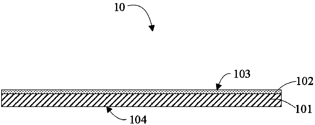
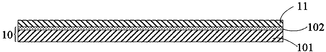
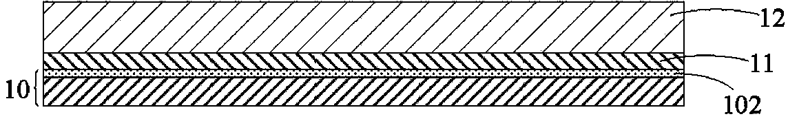
[0019] Step 1: See figure 1 , providing a single-sided blackened copper foil 10, the single-sided blackened copper foil 10 includes a copper body layer 101 and a first blackened layer 102, and the single-sided blackened copper foil 10 has an opposite first surface 103 and a second surface 104 , the first blackened layer 102 is formed on one side of the copper body layer 101 , and the surface of the first blackened layer 102 constitutes the first surface 103 of the single-sided blackened copper foil 10 . The first blackened layer 102 is formed after blackening treatment is performed...


PUM

PropertyMeasurementUnit
Thicknessaaaaaaaaaa
Thicknessaaaaaaaaaa

Abstract

The invention relates to a manufacturing method of a transparent printed circuit board. The method comprises the following steps: providing single-side blackening copper foil which includes a copper body layer and a first blackening layer formed at one side of the copper body layer; bonding a transparent substrate layer to the surface of the first blackening layer through a first colloid layer; performing blackening processing on the surface, which is opposite to the first blackening layer, of the single-side blackening copper foil so that the single-side blackening copper foil forms double-sided blackening copper foil; removing part of the double-sided blackening copper foil so as to making the double-sided blackening copper foil into a conductive line layer; and successively arranging a second colloid layer and a transparent coverage layer at one side, which is away from the transparent substrate layer, of the conductive line layer so as to form a transparent printed circuit board. The invention also relates to a transparent printed circuit board manufactured by use of the method.

Description

technical field [0001] The invention relates to circuit board manufacturing technology, in particular to a transparent printed circuit board and a manufacturing method thereof. Background technique [0002] Printed circuit boards have been widely used due to their advantages such as high assembly density. For the application of the circuit board, please refer to the literature Takahashi, A. Ooki, N. Nagai, A. Akahoshi, H. Mukoh, A. Wajima, M. Res. Lab, High density multilayer printed circuit board for HITAC M-880, IEEE Trans . on Components, Packaging, and Manufacturing Technology, 1992, 15(4): 1418-1425. [0003] Due to the personalization of electronic products, the requirements for printed circuit boards used in electronic products are becoming more and more diverse. At present, there is a transparent printed circuit board. The insulating substrate and cover film used to carry and protect the conductive circuit layer are transparent materials, and the internal conductiv...

Claims


Application Information

Patent Timeline
IPC IPC(8): H05K3/02H05K3/28H05K1/02
Inventor 何明展胡先钦钟佳宏陈怡岑
Owner AVARY HLDG (SHENZHEN) CO LTD
Why Eureka
Try Eureka