Protection method for inner circuit of printed circuit board

A technology for printed circuit boards and inner-layer circuits, applied in the directions of printed circuits, printed circuit manufacturing, and manufacturing of printed circuit precursors, etc., can solve the problems of longer process time, residual strippable ink, and increased material loss, so as to reduce defects. , The effect of increasing adhesion and saving material costs

Active Publication Date: 2014-06-11
SI FLEX
View PDF7 Cites 0 Cited by
  • Summary
  • Abstract
  • Description
  • Claims
  • Application Information

AI Technical Summary

Problems solved by technology

[0007] As mentioned above, since the peelable ink (Peelable Ink) is applied twice, the process time becomes longer, reducing productivity and increasing material loss
[0008] In addition, after printing the peelable ink (Peelable Ink), the outer layer

Method used


Image

  • Protection method for inner circuit of printed circuit board
  • Protection method for inner circuit of printed circuit board
  • Protection method for inner circuit of printed circuit board

Examples


Example Embodiment

[0030] Next, the inner layer circuit protection process of the printed circuit board of the present invention will be described in detail with reference to the accompanying drawings. The same structures or components in the drawings use the same reference signs as far as possible. In addition, the disclosed structures and functions that may confuse the focus of the present invention will not be repeated here.

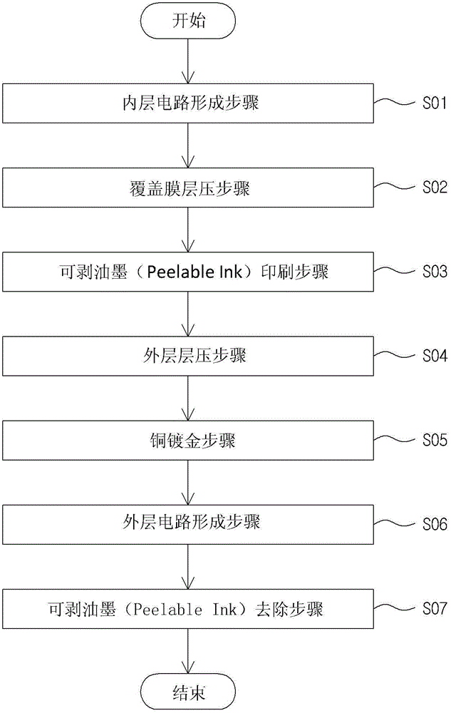
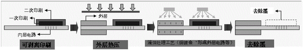
[0031] Figure 4 It is a schematic process diagram of the inner layer circuit protection process of the printed circuit board according to an embodiment of the present invention.

[0032] like Figure 4 As shown, the inner layer circuit protection process of the printed circuit board of the present invention is characterized in that, comprising: the inner layer circuit forming step S10, etching and removing the inner layer surface made of copper (Cu) to form the inner layer circuit; Pressing step S20, laminating and processing the upper part of the inner layer throug...


PUM


Abstract

A protection method for an inner circuit of a printed circuit board is provided. The protection method includes: a step (S10) of forming the inner circuit; a step (S20) of laminating a coverlay; a step (S30) of laminating an outer layer; a step (S40) of printing a peelable ink; a step (S50) of performing copper plating; a step (S60) of forming an outer layer circuit; and a step (S70) of removing the peelable ink. The protection method enables shielding with one ink application, and therefore the cohesive power of the peelable ink is increased by performing thermal compression bonding after the printing of peelable ink, thus preventing liquid from permeating into a circuit in a liquid process.

Description

technical field [0001] The present invention relates to the inner layer circuit protection process of printed circuit boards, in particular to printing peelable ink (Peelable Ink) on the upper part of the inner layer circuit to be protected after laminating the outer layer on the upper part of the inner layer with a hot press (hot press) , thereby reducing the printing times of the above-mentioned peelable ink (Peelable Ink), and preventing the inner layer circuit protection process of the printed circuit board where the ink remains due to the operation of the above-mentioned outer layer hot press (hot press). Background technique [0002] Now, in the process of manufacturing MLB (MULTI-LAYER BOARD) of R / F TYPE (RIGID / FLEXIBLE TYPE), manufacturers of F.PCB protect the inner layer (FLEXIBLE Layer) circuit and use two peelable inks to protect the inner layer circuit. [0003] The above-mentioned Peelable Ink is a material used in the printing process that can be peeled off by...

Claims


Application Information

Patent Timeline
IPC IPC(8): H05K3/28
CPCH05K3/022H05K3/06H05K3/12H05K3/281H05K3/429
Inventor 李大元徐正植李成基赵承薰
Owner SI FLEX
Why Eureka
Try Eureka