Semiconductor device, manufacturing method thereof, and power supply device
A manufacturing method and semiconductor technology, applied in the fields of semiconductor/solid-state device manufacturing, semiconductor devices, circuits, etc., can solve problems such as reduced withstand voltage, and achieve the effect of reducing manufacturing costs and process man-hours
- Summary
- Abstract
- Description
- Claims
- Application Information
AI Technical Summary
Problems solved by technology
Method used
Image


Examples
no. 1 Embodiment approach 〕
[0046] First, for the semiconductor device and its manufacturing method of the present embodiment, refer to figure 1 ~ Figure 7 (C) for illustration.
[0047] The semiconductor device of the present embodiment is a high-voltage, high-speed-operable semiconductor device using a GaN-based semiconductor, for example, a GaN-based Schottky barrier diode (GaN-based electronic device).
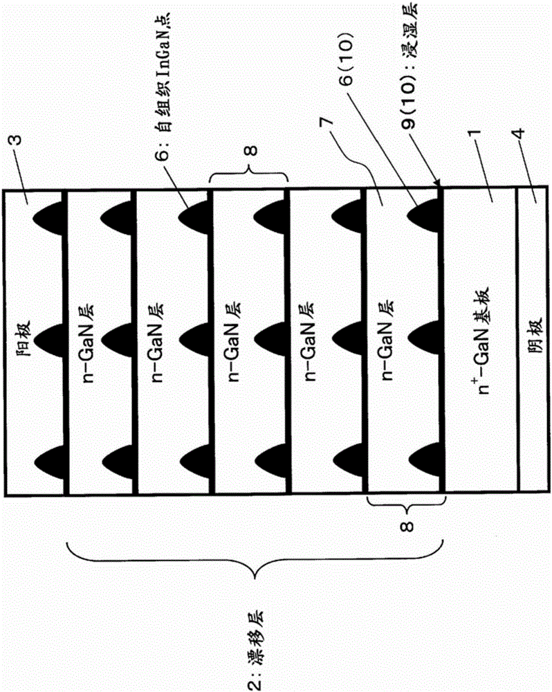
[0048] This GaN-based Schottky barrier diode such as figure 1 As shown, there are: an n-type GaN substrate 1; a drift layer 2 disposed on the n-type GaN substrate 1; an anode electrode 3 connected to the drift layer 2 Schottky; a cathode electrode disposed on the back side of the n-type GaN substrate 1 4.
[0049] In this case, n-type GaN substrate 1 is provided on the side of drift layer 2 opposite to the side on which anode electrode 3 is provided. Further, cathode electrode 4 is provided on the side of n-type GaN substrate 1 opposite to the side on which drift layer 2 is provided.
[0050]In...
no. 2 Embodiment approach 〕
[0082] Next, for the semiconductor device and its manufacturing method of the present embodiment, refer to Figure 8 ~ Figure 1 1(C) for clarification.
[0083] The semiconductor device of the present embodiment is a high withstand voltage and high-speed operable semiconductor device using a GaN-based semiconductor, for example, a GaN-based vertical transistor (GaN-based electronic device; for example, UMOSFET: U-shaped trench metal oxide semiconductor field effect transistor).
[0084] This GaN-based vertical transistor such as Figure 8 As shown, it has: n-type GaN substrate 1; n-type GaN buffer layer 5; InGaN point buried drift layer 2; p-type GaN body layer 20 (p-type semiconductor layer); n-type GaN contact layer 21; source electrode 22; Drain electrode 23; Gate electrode 24. Also, a stacked structure of n-type GaN buffer layer 5 , InGaN dot-buried drift layer 2 , p-type GaN body layer 20 , and n-type GaN contact layer 21 is referred to as semiconductor stacked structur...
no. 3 Embodiment approach 〕
[0101] Next, for the semiconductor device and its manufacturing method of the present embodiment, refer to Figure 12 ~ Figure 1 4 for explanation.
[0102] The semiconductor device of the present embodiment has the GaN-based Schottky barrier diode (GaN-based electronic device) of the first embodiment described above and the GaN-based vertical transistor (GaN-based electronic device) of the second embodiment described above on the same substrate. Semiconductor devices such as UMOSFET).
[0103] That is, the present semiconductor device such as Figure 12 As shown, a GaN-based Schottky barrier diode region 30 and a GaN-based vertical transistor region 31 are included.
[0104] Here, the GaN-based Schottky barrier diode region 30 has: an n-type GaN substrate 1; an n-type GaN buffer layer 5; an InGaN dot-buried drift layer 2; an anode electrode 3 that is Schottky-jointed with the drift layer 2; Cathode electrode 4 on the back side of n-type GaN substrate 1 . Furthermore, n-ty...
PUM
 Abstract
Description
Claims
Application Information
 - R&D
- Intellectual Property
- Life Sciences
- Materials
- Tech Scout
- Unparalleled Data Quality
- Higher Quality Content
- 60% Fewer Hallucinations
Browse by: Latest US Patents, China's latest patents, Technical Efficacy Thesaurus, Application Domain, Technology Topic, Popular Technical Reports.
© 2025 PatSnap. All rights reserved.Legal|Privacy policy|Modern Slavery Act Transparency Statement|Sitemap|About US| Contact US: help@patsnap.com