
Protruding point of package substrate and manufacturing method of protruding point

A technology for packaging substrates and manufacturing methods, which is applied in semiconductor/solid-state device manufacturing, semiconductor/solid-state device parts, semiconductor devices, etc. Difficult control, great impact on assembly, etc., to achieve good welding performance, good consistency, and increased capacity

Active Publication Date: 2014-10-08
NAT CENT FOR ADVANCED PACKAGING
View PDF4 Cites 0 Cited by
  • Summary
  • Abstract
  • Description
  • Claims
  • Application Information

AI Technical Summary

Problems solved by technology

Usually, this electroplating process needs to connect the electrodes of all electroplating bumps together through wires to form electroplating lines. After electroplating the bumps, all the electroplating lines need to be etched away before the quality inspection of the substrate can be carried out; the process is complex, It is difficult to control the height of plating bumps
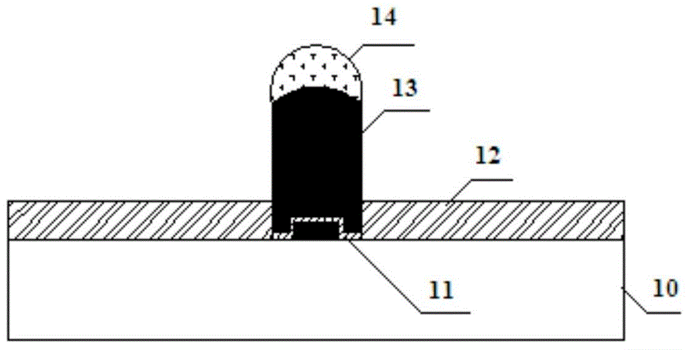
[0003] see figure 1 , In the existing bump structure, the appearance shape of the bump has a great influence on the subsequent assembly. If the shape of the copper bump is consistent, the height and shape consistency will be very good after solder reflow. If the shape is inconsistent, the solder height will be stable. There will be problems, and the overall flattening treatment is required. Therefore, the consistency and surface morphology of the electroplated copper bumps are relatively high.

Method used


Image

  • Protruding point of package substrate and manufacturing method of protruding point
  • Protruding point of package substrate and manufacturing method of protruding point
  • Protruding point of package substrate and manufacturing method of protruding point

Examples


Embodiment Construction

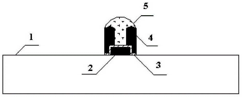
[0023] see figure 2 , the embodiment of the present invention provides a bump, including: a bump body 4; the bump body 4 is a cylindrical structure; the bump body 4 is located on the electroless copper plating layer 3 above the inner circuit 2. The solder 5 with a low melting point is filled in the inner cavity of the bump body 4, thereby increasing the amount of the solder 5 and ensuring the stability of soldering. On the other hand, when the low melting point solder 5 is filled in the inner cavity of the bump body 4, it is constrained by the bump wall and the surface tension of the fluid solder itself to form a stable and regular spherical surface, thereby ensuring the smoothness of the bump body 4. Consistency in height and shape is good.

[0024] The center of the bottom of the bump body 4 coincides with the center line of the inner layer circuit; thereby ensuring that the bump body 4 can form a stable connection with the inner layer circuit 2 from the side and upper sur...


PUM


Abstract

The invention belongs to the technical field of integrated circuit package and discloses a manufacturing method of a protruding point of a package substrate. The method comprises the steps that an inter-layer circuit is manufactured on the package substrate; electroless copper plating is conducted on the surface of the package substrate; electroplating is conducted on an electroless copper plating layer over the inter-layer circuit so that the cylindrical protruding point can be formed; the portions, outside the range of the protruding point and at the bottom of an inner cavity of the protruding point, of the electroless copper plating layer are etched; the inner wall of the protruding point is filled with low-melting-point solder. The protruding point is directly manufactured on the inner-layer copper circuit, operation complexity is reduced, and the technological process is simplified; meanwhile, the height of the cylindrical protruding point is easy to control and consistency is good; the solder capacity is large and the soldering performance is good.

Description

technical field [0001] The invention relates to the technical field of integrated circuit packaging, in particular to a bump of a packaging substrate and a manufacturing method thereof. Background technique [0002] In the process of electroplating bumps, since bump electroplating is completed in a dry film pattern with a high aspect ratio, it is difficult to obtain a flat pattern structure on the top of the bumps due to the small aperture of the bump window after the bumps are formed after electroplating. Usually, this electroplating process needs to connect the electrodes of all electroplating bumps together through wires to form electroplating lines. After electroplating the bumps, all the electroplating lines need to be etched away before the quality inspection of the substrate can be carried out; the process is complex, Plating bump height control is difficult. [0003] see figure 1 , In the existing bump structure, the appearance shape of the bump has a great influen...

Claims


Application Information

Patent Timeline
Patent Type & Authority Applications(China)
IPC IPC(8): H01L23/488H01L21/48
CPCH01L2224/11
Inventor 于中尧孙瑜方志丹
Owner NAT CENT FOR ADVANCED PACKAGING
Learn More