Ag alloy film to be used as reflecting film and/or transmitting film or as electrical wiring and/or electrode, ag alloy sputtering target, and ag alloy filler
A technology of electrical wiring and alloy film, applied in the field of Ag alloy film used for reflective film and/or transmissive film, or used for electrical wiring and/or electrode, and Ag alloy sputtering target and Ag alloy filler, can solve the problem of Excellent durability, excellent adhesion, and excellent productivity are achieved without problems such as cloudiness
- Summary
- Abstract
- Description
- Claims
- Application Information
AI Technical Summary
Problems solved by technology
Method used
Image


Examples
Embodiment 1
[0056] On a glass substrate (Dow Corning's non-alkali glass #1737, diameter: 50 mm, thickness: 0.7 mm), a pure Ag film or an Ag film having the composition shown in Table 1 was formed by sputtering using a DC magnetron sputtering device. Alloy films (both film thicknesses are 100nm, single-layer film) are formed. The film-forming conditions at this time are as follows.
[0057] (film forming conditions)
[0058] Substrate temperature: room temperature
[0059] Film forming power: DC15W / cm 2
[0060] Ar pressure: 1~3mTorr
[0061] Electrode spacing: 55mm
[0062] Film forming speed: 7.0~8.0nm / sec
[0063] Ultimate vacuum degree: 1.0×10 -5 Below Torr
[0064] In addition, in the above film formation, as a sputtering target, a pure Ag target (when forming a pure Ag film) or an Ag alloy having the same composition as the film composition shown in the following Table 1 prepared by a vacuum melting method was used. Sputtering targets (targets all 4 inches in diameter). In ...
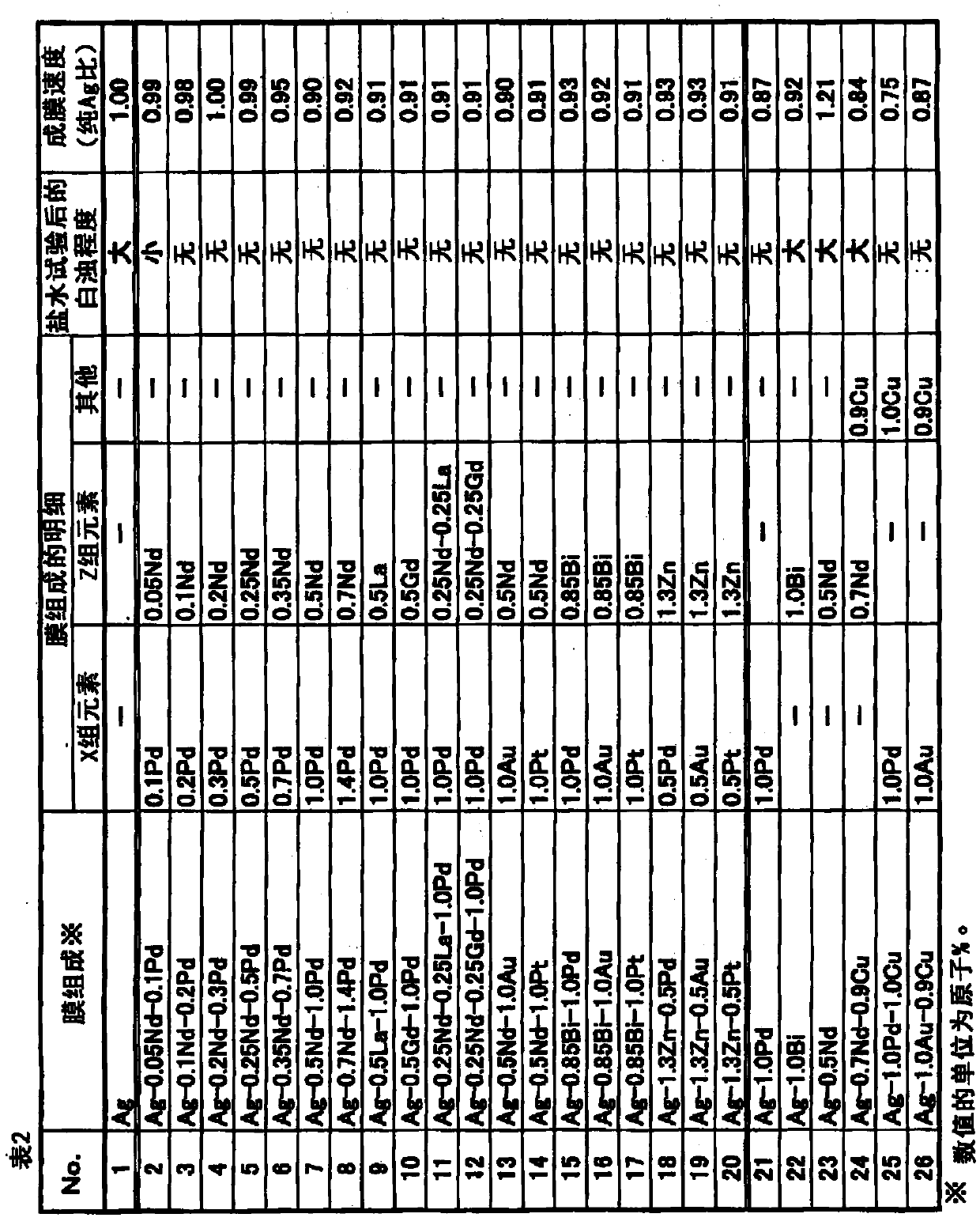
Embodiment 2
[0083] On a glass substrate (Dow Corning's non-alkali glass #1737, diameter: 50 mm, thickness: 0.7 mm), use a DC magnetron sputtering device to form a pure Ag film or an Ag alloy with the composition shown in Table 2 by sputtering. Films (both film thicknesses are 100nm, single-layer film) are formed into films. The film-forming conditions at this time are as follows.
[0084] (film forming conditions)
[0085] Substrate temperature: room temperature
[0086] Film forming power: DC2.55W / cm 2
[0087] Ar gas pressure: 1.9Pa
[0088] Electrode spacing: 120mm
[0089] Ultimate vacuum degree: 4.0×10 -5 Below Pa
[0090] In addition, in the above film formation, as the sputtering target, a pure Ag target (in the case of forming a pure Ag film) or an Ag alloy having the same composition as the film composition shown in Table 2 below prepared by a vacuum melting method was used. Sputtering targets (targets all 4 inches in diameter). In addition, in No. 15-17 and 22 of Table ...
PUM
| Property | Measurement | Unit |
|---|---|---|
| diameter | aaaaa | aaaaa |
| thickness | aaaaa | aaaaa |
| thickness | aaaaa | aaaaa |
Abstract
Description
Claims
Application Information
 - R&D
- Intellectual Property
- Life Sciences
- Materials
- Tech Scout
- Unparalleled Data Quality
- Higher Quality Content
- 60% Fewer Hallucinations
Browse by: Latest US Patents, China's latest patents, Technical Efficacy Thesaurus, Application Domain, Technology Topic, Popular Technical Reports.
© 2025 PatSnap. All rights reserved.Legal|Privacy policy|Modern Slavery Act Transparency Statement|Sitemap|About US| Contact US: help@patsnap.com