Supercharge Your Innovation With Domain-Expert AI Agents!

Internal plasma grids for semiconductor manufacturing

A plasma and semiconductor technology, applied in the field of plasma grids, can solve problems such as difficult to achieve multiple purposes

Active Publication Date: 2017-05-10
LAM RES CORP
View PDF9 Cites 0 Cited by
  • Summary
  • Abstract
  • Description
  • Claims
  • Application Information

AI Technical Summary

Problems solved by technology

[0008] Multiple objectives such as those articulated above have been found to be difficult to achieve when etching advanced structures such as FinFET gates

Method used


Image

  • Internal plasma grids for semiconductor manufacturing
  • Internal plasma grids for semiconductor manufacturing
  • Internal plasma grids for semiconductor manufacturing

Examples


Embodiment Construction

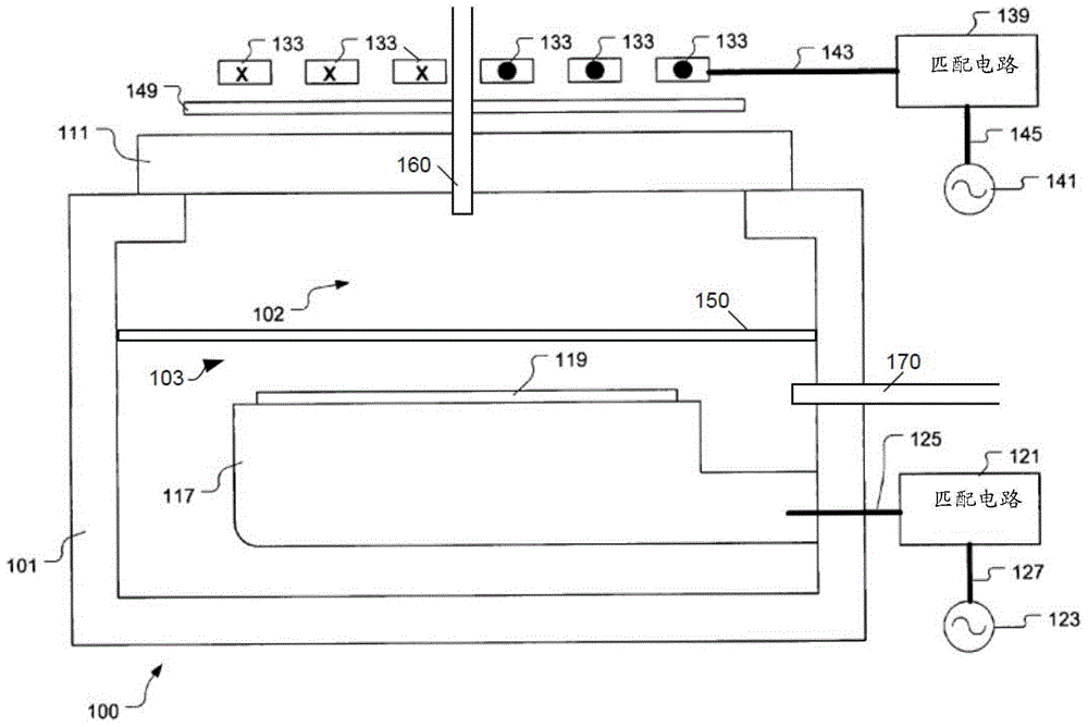
[0028] In this specification, the terms "semiconductor wafer," "wafer," "substrate," "wafer substrate," and "partially fabricated integrated circuit" are used interchangeably. It will be understood by those of ordinary skill in the art that the term "partially fabricated integrated circuit" may refer to devices on a semiconductor wafer during any of the different stages of integrated circuit fabrication on the semiconductor wafer. The following detailed description assumes that the present invention is implemented on a wafer. Exemplary workpieces (sometimes referred to as standard semiconductor substrates) include 200, 300, and 450 mm diameter semiconductor substrates. However, the present invention is not limited thereto. Workpieces can be formed in a variety of shapes, sizes and materials.

[0029] In the following description, numerous specific details are set forth in order to provide a thorough understanding of the present invention. However, the present invention may ...


PUM


Abstract

Embodiments disclosed herein relate to internal plasma grids for semiconductor manufacturing, and in particular to improved methods and apparatus for etching semiconductor substrates. A plasma grid is positioned in the reaction chamber to divide the chamber into upper and lower sub-chambers. The plasma grid may have specific aspect ratio slots to allow certain species to pass from the upper subchamber to the lower subchamber. In some cases, an electron-ion plasma is generated in the upper subchamber. Electrons passing through the grid to the lower subchamber are cooled as they pass. In some cases, this results in an ion-ion plasma in the lower subchamber. The plasma in the lower subchamber has a lower electron density, lower electron effective temperature and higher negative ion:positive ion ratio than the plasma in the upper subchamber. The disclosed embodiments may result in an etch process with good center-to-edge uniformity, selectivity, profile angle, and Iso / dense loading.

Description

[0001] Cross References to Related Applications [0002] This application claims priority to U.S. Patent Application No. 14 / 082,009, filed June 12, 2013, entitled "INTERNAL PLASMA GRID FORSEMICONDUCTOR FABRICATION," which claims priority on April 5, 2013 Priority to U.S. Provisional Application No. 61 / 809,246, entitled "INTERNAL PLASMA GRID FORSEMICONDUCTOR FABRICATION," filed on , each of which is hereby incorporated by reference in its entirety for all purposes. technical field [0003] The present invention relates generally to the field of semiconductor fabrication technology, and more particularly to internal plasma grids for semiconductor fabrication. Background technique [0004] One operation frequently employed in semiconductor production is an etching operation. In an etching operation, one or more materials are partially or completely removed from a partially fabricated integrated circuit. Plasma etching is frequently used, especially where the geometries involv...

Claims


Application Information

Patent Timeline
Patent Type & Authority Patents(China)
IPC IPC(8): H01J37/02H01J37/305H01L21/3065
CPCH01J37/32422H01J37/32633H01J37/32009H01J37/3244H01J37/32715H01L21/3065H01L21/31116H01L21/31138H01L21/32136H01L21/67069H01J2237/334
Inventor 亚历克斯·帕特森哈梅特·辛格理查德·A·马什索斯藤·利尔瓦希德·瓦赫迪吴英萨拉瓦纳普里亚·西里拉曼
Owner LAM RES CORP
Features
  • R&D
  • Intellectual Property
  • Life Sciences
  • Materials
  • Tech Scout
  • Unparalleled Data Quality
  • Higher Quality Content
  • 60% Fewer Hallucinations
Learn More