LED module and production method therefor, lighting device
A technology of LED modules and LED chips, which is applied to lighting devices, lighting and heating equipment, semiconductor devices of light-emitting elements, etc., can solve the problems of reducing light extraction efficiency, etc., and achieve the effect of improving light extraction efficiency and improving light extraction efficiency.
- Summary
- Abstract
- Description
- Claims
- Application Information
AI Technical Summary
Problems solved by technology
Method used
Image

Examples
Embodiment 1
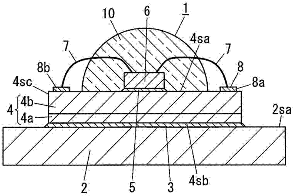
[0080] In the following, reference will be made to Figures 1 to 8 The LED module 1 of this embodiment is described.
[0081] The LED module 1 includes: a base 4 having a face 4sa in the thickness direction of the base 4; an LED chip 6 bonded to the face 4sa of the base 4 with the first bonding portion 5; Wiring circuit (patterned conductor) 8 .
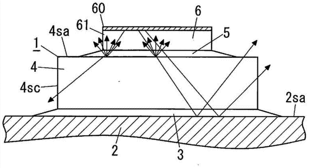
[0082] In the LED module 1 , the first bonding portion 5 allows the light emitted from the LED chip 6 to pass therethrough, and the base 4 is a light-transmitting member having light-diffusing properties. The translucent member propagates incident light to the outside by refraction or internal diffusion (scattering).
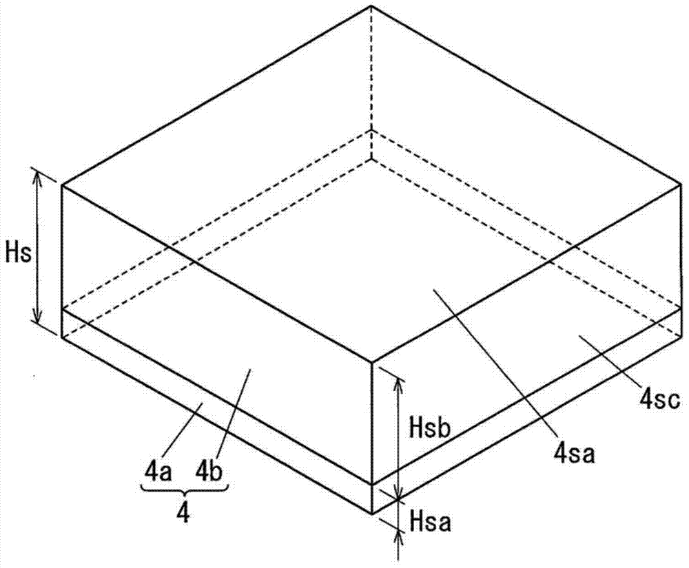
[0083] The plane size of the base 4 is larger than the plane size of the LED chip 6 . A patterned wiring circuit 8 is provided on the face 4 sa of the submount 4 to avoid overlapping with the LED chip 6 . The base 4 is composed of at least two transparent layers stacked in the thickness direction of the base 4 . T...
Embodiment 2
[0237] The LED module 1 of this embodiment differs from the LED module 1 of Embodiment 1 in that, as Figure 32As shown in A, 32B and 32C, the base 4 has an elongated shape and includes a plurality of LED chips 6 . Note that constituent elements similar to those in Embodiment 1 have the same reference numerals, and repeated description thereof will be omitted.
[0238] In the LED module 1, along a predetermined direction on the surface 4sa of the base 4 ( Figure 32 The horizontal direction in B) aligns a plurality of LED chips 6 . In the LED module 1 , the LED chips 6 aligned in a prescribed direction and the wires 7 connected to the corresponding LED chips 6 are covered with a strip-shaped color conversion portion 10 . The color conversion portion 10 has a concave portion 10b to suppress total reflection of light emitted from each LED chip 6 between LED chips 6 adjacent to each other in a prescribed direction.
[0239] The patterned wiring circuit 8 serving as a circuit i...
Embodiment 3
[0304] In the following, reference will be made to Figures 37 to 39 The LED module 1 of this embodiment is described.
[0305] The LED module 1 of this embodiment is different from the LED module 1 of Embodiment 2 in that the base 4 has a square shape, and a plurality of (36 in the example in the figure) LED chips 6 are arranged in a two-dimensional array. Note that constituent elements similar to those in Embodiment 2 have the same reference numerals, and repeated description thereof will be omitted.
[0306] The LED module 1 comprises a plurality of LED chips 6 on the face 4 sa of the submount 4 . The patterned wiring circuit 8 includes a first conductor 8 a and a second conductor 8 b arranged independently from each other on the surface 4 sa of the base 4 . In the LED module 1, the plurality of LED chips 6 includes a group of LED chips 6 connected in series and arranged on an imaginary line M1 connecting the first conductor 8a and the second conductor 8b to each other. ...
PUM
| Property | Measurement | Unit |
|---|---|---|
| Grain diameter | aaaaa | aaaaa |
| Thickness | aaaaa | aaaaa |
| Wavelength | aaaaa | aaaaa |
Abstract
Description
Claims
Application Information
 - R&D Engineer
- R&D Manager
- IP Professional
- Industry Leading Data Capabilities
- Powerful AI technology
- Patent DNA Extraction
Browse by: Latest US Patents, China's latest patents, Technical Efficacy Thesaurus, Application Domain, Technology Topic.
© 2024 PatSnap. All rights reserved.Legal|Privacy policy|Modern Slavery Act Transparency Statement|Sitemap