Silicon-based avalanche photodetector taking fluorinated graphene as insulating layer and preparation method
A technology of fluorinated graphene and avalanche optoelectronics, which is applied in the field of photoelectric detection, can solve problems affecting device noise, etc., achieve high optical response, improve time response, and eliminate dead layers.
- Summary
- Abstract
- Description
- Claims
- Application Information
AI Technical Summary
Benefits of technology
Problems solved by technology
Method used
Image
Examples
Embodiment 1
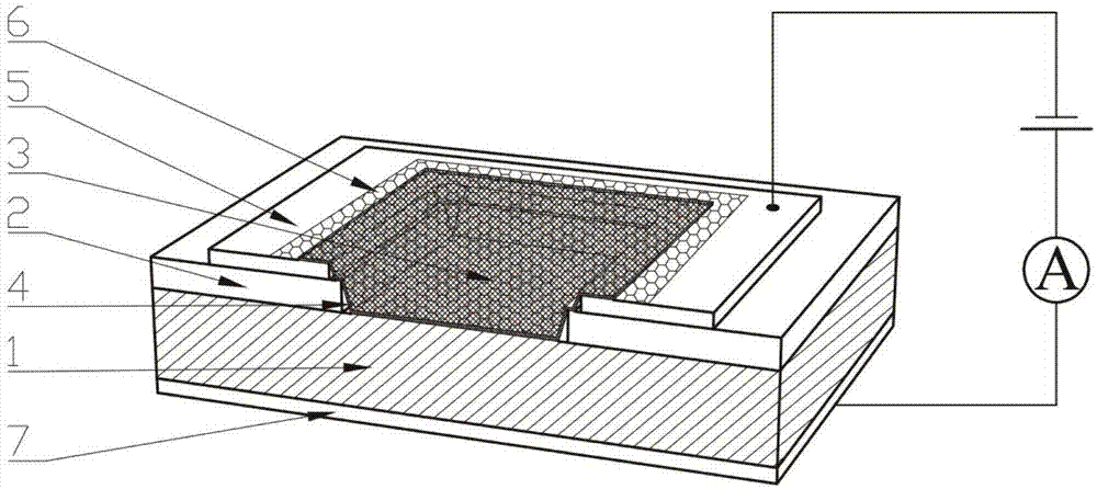
[0037] Embodiment 1: the preparation steps of the avalanche photodetector with fluorinated graphene as the insulating layer are as follows:
[0038] (1) On the upper surface of n-type silicon substrate 1, silicon dioxide spacer layer 2 is oxidized and grown, and the resistivity of n-type silicon substrate 1 used is 1~10Ω·cm; The thickness of silicon dioxide spacer layer 2 is 300nm~ 500nm, the growth temperature is 900~1200℃;
[0039] (2) Photoetch the top electrode 5 pattern on the surface of the silicon dioxide isolation layer 2, and then use electron beam evaporation technology to first grow a chromium adhesion layer with a thickness of about 5 nm, and then grow a 50 nm gold electrode;
[0040] (3) On the surface of the silicon dioxide spacer layer 2 grown with the top electrode 5, the silicon dioxide window 3 pattern is photoetched, and then by reactive ion etching technology, using C 4 f 8 Plasma etching the silicon dioxide isolation layer 2 and removing residual silicon...
Embodiment 2
[0047] Embodiment 2: the specific steps of the avalanche photodetector with fluorinated graphene as insulating layer are:
[0048] Steps (1), (2), (3) and (4) are the same as in Example 1.
[0049] (5) preparing and transferring the fluorinated graphene insulating layer 4; the specific steps are as follows:
[0050] (5.1) on the upper surface of top electrode 5, top electrode 5, silicon dioxide spacer 2 and n-type silicon substrate 1 surround the inner surface transfer graphene film 6 of the trapezoidal space that forms; Wherein, transfer graphene film 6 Method is identical with the method for transferring fluorinated graphene insulating layer 4 in embodiment 1 step (5);
[0051] (5.2) The graphene film described in step (5.1) is fluorinated: the sample that transfers the graphene film 6 is put into the vacuum chamber of reactive ion etching system, adopts sulfur hexafluoride (SF 6 ) plasma to fluorinate the surface of the graphene film 6 to form a fluorinated graphene insul...
PUM
| Property | Measurement | Unit |
|---|---|---|
| Resistivity | aaaaa | aaaaa |
| Thickness | aaaaa | aaaaa |
| Thickness | aaaaa | aaaaa |
Abstract
Description
Claims
Application Information
 - R&D Engineer
- R&D Manager
- IP Professional
- Industry Leading Data Capabilities
- Powerful AI technology
- Patent DNA Extraction
Browse by: Latest US Patents, China's latest patents, Technical Efficacy Thesaurus, Application Domain, Technology Topic, Popular Technical Reports.
© 2024 PatSnap. All rights reserved.Legal|Privacy policy|Modern Slavery Act Transparency Statement|Sitemap|About US| Contact US: help@patsnap.com


