V waveband microstrip probe type waveguide microstrip switching circuit and parameter design method

A waveguide microstrip conversion and microstrip probe technology, which is applied in the fields of electrical digital data processing, calculation, special data processing applications, etc., can solve the problems of complex process realization, deviation of design results, large structure size, etc., and achieve accurate calculation results. , the effect of small insertion loss

Inactive Publication Date: 2015-02-04
HUADONG PHOTOELECTRIC TECHN INST OF ANHUI PROVINCE
View PDF2 Cites 5 Cited by
  • Summary
  • Abstract
  • Description
  • Claims
  • Application Information

AI Technical Summary

Problems solved by technology

The coaxial probe type waveguide microstrip conversion circuit is easy to design and is a relatively mature circuit form, but it also has the following disadvantages: (1) The structure size is large; (2) The cost is high; (3) The process is realized more complex
Generally, in solid-state circuits with low frequency (below the Ka band), coaxial probe type waveguide microstrip conversion circuits are widely used, but when the operating frequency rises to the V band, high-performance coaxial probes are not easy to manufacture, and the price The cost is high; and

Method used


Image

  • V waveband microstrip probe type waveguide microstrip switching circuit and parameter design method
  • V waveband microstrip probe type waveguide microstrip switching circuit and parameter design method
  • V waveband microstrip probe type waveguide microstrip switching circuit and parameter design method

Examples


Example Embodiment

[0037] In order to make the objectives, technical solutions and advantages of the present invention clearer, the following further describes the present invention in detail with reference to the accompanying drawings and embodiments. It should be understood that the specific embodiments described herein are only used to explain the present invention, but not to limit the present invention.

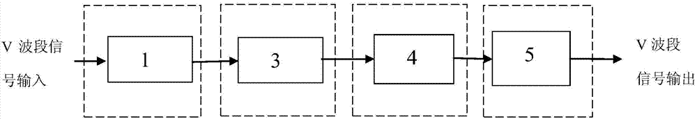
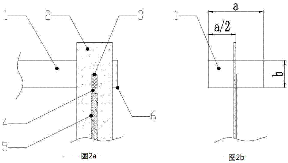
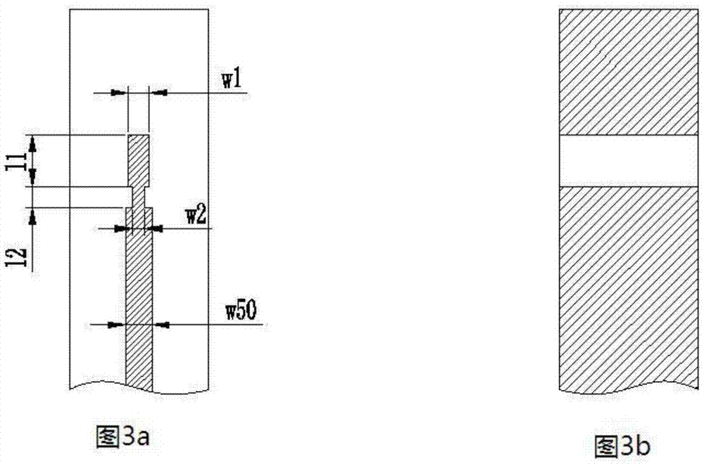
[0038] Refer to figure 1 , The present invention includes rectangular waveguide 1, microstrip probe 3, quarter impedance conversion line 4 and 50 ohm microstrip transmission line 5, including microstrip probe 3, quarter impedance conversion line 4 and 50 ohm microstrip The transmission line 5 is made on the same dielectric substrate 2. The V-band millimeter wave signal is input from the rectangular waveguide port 1, the mode is converted through the microstrip probe 3 and the quarter impedance conversion line 4, and finally transmitted and output from the 50 ohm transmission line 5.

[0039] ...


PUM

PropertyMeasurementUnit
Lengthaaaaaaaaaa
Widthaaaaaaaaaa
Lengthaaaaaaaaaa

Abstract

The invention discloses a V waveband microstrip probe type waveguide microstrip switching circuit. The circuit comprises a rectangular waveguide (1), a dielectric substrate (2), a microstrip probe (3), a quarter impedance conversion line (4) and a 50 ohm microstrip transmission line (5), wherein the microstrip probe (3), the quarter impedance conversion line (4) and the 50 ohm microstrip transmission line (5) are arranged on the dielectric substrate (2), the bottom surface of the dielectric substrate (2) is welded on the rectangular waveguide (1), the thickness of the dielectric substrate (2) is 5 mil, and the bottom surface on the dielectric substrate (2), on which the microstrip probe (3) is, is made of an insulated material. According to the design of the switching circuit, non-dominant mode model radiation of a microwave signal in transmission in the rectangular waveguide is fully taken into account, and the switching circuit also combines the latest three-dimensional electromagnetic field simulation software, so that the computing result is more precise, and the manufacture of circuit boards can be better instructed.

Description

technical field [0001] The invention relates to a V-band waveguide microstrip conversion circuit, in particular to a V-band microstrip probe type waveguide microstrip conversion circuit. Background technique [0002] With the development of microwave and millimeter wave technology, microwave and millimeter wave hybrid integrated circuits are widely used in military radar, guidance and other weapon combat readiness systems, as well as in civilian communications and automobile collision avoidance systems. In order to minimize the transmission loss in the millimeter-wave frequency band, most of the external interfaces of the V-band millimeter-wave solid-state circuit adopt a waveguide structure. Therefore, the waveguide-microstrip conversion circuit is undoubtedly a key component in the millimeter-wave system. Affect the technical indicators of the whole machine. [0003] According to the circuit type, the waveguide microstrip conversion circuit is divided into the following c...

Claims


Application Information

Patent Timeline
IPC IPC(8): G06F17/50
Inventor 陈在陈兴盛朱良凡蔡庆钢
Owner HUADONG PHOTOELECTRIC TECHN INST OF ANHUI PROVINCE
Why Eureka
Try Eureka