Patterned substrate and preparation method thereof, epitaxial-wafer preparation method and epitaxial wafer
A patterned substrate and epitaxial wafer technology, applied in the field of epitaxial wafers, can solve the problems of low light reflectivity and achieve the effects of increasing light reflectivity, improving light extraction efficiency, and improving light extraction efficiency
- Summary
- Abstract
- Description
- Claims
- Application Information
AI Technical Summary
Problems solved by technology
Method used
Image

Examples
Example Embodiment
[0041] Example one
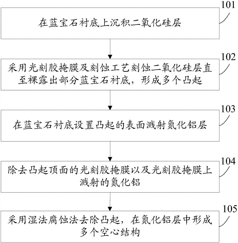
[0042] The embodiment of the present invention provides a method for preparing a patterned substrate, see figure 1 , The method includes:
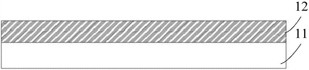
[0043] Step 101: Deposit a silicon dioxide layer on a sapphire substrate.
[0044] In this embodiment, depositing a silicon dioxide layer on a sapphire substrate includes:
[0045] A plasma-enhanced chemical vapor deposition method or a sol-gel method is used to deposit a silicon dioxide layer on the sapphire substrate.
[0046] Such as figure 2 As shown, a silicon dioxide layer 12 is deposited on the sapphire substrate 11.
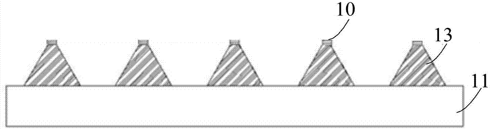
[0047] Step 102: Use a photoresist mask and an etching process to etch the silicon dioxide layer until a part of the sapphire substrate is exposed to form a plurality of protrusions. The protrusions have a mesa structure and a photoresist mask is left on the top surface of the protrusions. membrane.
[0048] Specifically, the protrusion may be one or more of a truncated cone structure, an elliptical cone st...
Example Embodiment
[0065] Example two
[0066] The embodiment of the present invention provides a method for manufacturing an epitaxial wafer, see Figure 7 , The method includes:
[0067] Step 201: Prepare a patterned substrate according to the method in the first embodiment.
[0068] Step 202: sequentially growing an n-type gallium nitride layer, a multiple quantum well layer and a p-type gallium nitride layer on the patterned substrate to form an epitaxial wafer.
[0069] Specifically, the side epitaxial growth method is used to sequentially grow an n-type gallium nitride layer, a multiple quantum well layer, and a p-type gallium nitride layer on a patterned substrate to form an epitaxial wafer.
[0070] In the embodiment of the present invention, a silicon dioxide layer is deposited on a sapphire substrate, a plurality of protrusions are etched using a photoresist mask and an etching process, and an aluminum nitride layer is sputtered on the surface of the sapphire substrate. The protrusions are remo...
Example Embodiment
[0071] Example three
[0072] The embodiment of the present invention provides a patterned substrate, see Figure 8 , The substrate includes:
[0073] A sapphire substrate 301 and an aluminum nitride layer 302 disposed on the sapphire substrate 301. A plurality of hollow structures 302a are provided in the aluminum nitride layer 302, and the hollow structures 302a are mesa structures.
[0074] Specifically, the hollow structure 302a may be one or more of a truncated cone structure, an elliptical cone structure, and a prism cone structure.
[0075] Further, the radius or width of the top surface of the hollow structure 302a is 0.05-0.5um, the radius or width of the bottom surface of the hollow structure 302a is 0.5-10um, and the height of the hollow structure 302a is 0.5-5um. The hollow structure of this size has an obvious effect on reflectivity and can maximize the efficiency of LED light.
[0076] In this embodiment, a plurality of hollow structures 302a are arranged in a matrix to f...
PUM
 Abstract
Description
Claims
Application Information
 - R&D Engineer
- R&D Manager
- IP Professional
- Industry Leading Data Capabilities
- Powerful AI technology
- Patent DNA Extraction
Browse by: Latest US Patents, China's latest patents, Technical Efficacy Thesaurus, Application Domain, Technology Topic.
© 2024 PatSnap. All rights reserved.Legal|Privacy policy|Modern Slavery Act Transparency Statement|Sitemap