Interposer, manufacturing method, packaging structure and bonding method for interposer
A packaging structure and adapter board technology, which is applied in printed circuit manufacturing, stacking printed circuit boards, stacking and separating printed circuit boards, etc., can solve problems such as low bonding strength, low bonding reliability, and small contact area
- Summary
- Abstract
- Description
- Claims
- Application Information
AI Technical Summary
Problems solved by technology
Method used
Image

Examples
Embodiment Construction
[0033] Specific embodiments of the present invention will be described in detail below in conjunction with the accompanying drawings. It should be understood that the specific embodiments described here are only used to illustrate and explain the present invention, and are not intended to limit the present invention.
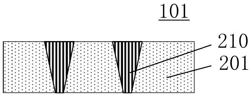
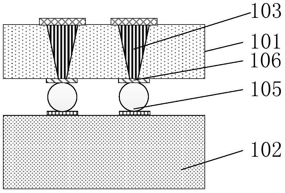
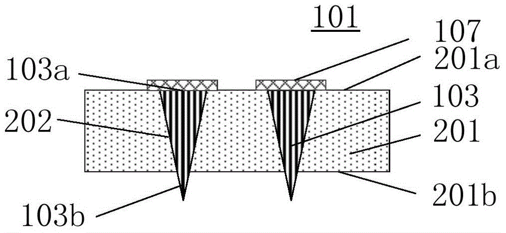
[0034] Figure 2a and Figure 2b It is a schematic diagram of the adapter plate provided by the two embodiments of the present invention. Such as Figure 2a In the illustrated embodiment, the adapter board 101 may include a board body 201 , a tapered conductor 103 and a wiring structure 107 . The plate body 201 may have a first surface 201 a and a second surface 201 b opposite to each other, and a frustum-shaped through hole 202 penetrating through the plate body 201 may be formed between the first surface 201 a and the second surface 201 b. A tapered conductor 103 can be filled in the frustum-shaped through hole 202, the tapered conductor 103 has a planar e...
PUM
 Abstract
Description
Claims
Application Information
 - R&D
- Intellectual Property
- Life Sciences
- Materials
- Tech Scout
- Unparalleled Data Quality
- Higher Quality Content
- 60% Fewer Hallucinations
Browse by: Latest US Patents, China's latest patents, Technical Efficacy Thesaurus, Application Domain, Technology Topic, Popular Technical Reports.
© 2025 PatSnap. All rights reserved.Legal|Privacy policy|Modern Slavery Act Transparency Statement|Sitemap|About US| Contact US: help@patsnap.com