Electroplating method with uniform plating thickness and products thereof
A coating thickness, uniform technology, applied in the direction of coating, circuit, printed circuit, etc., can solve the problem of different current density and achieve the effect of uniform thickness
- Summary
- Abstract
- Description
- Claims
- Application Information
AI Technical Summary
Problems solved by technology
Method used
Image

Examples
Embodiment Construction
[0026] The present invention will be described in detail below in conjunction with the accompanying drawings and embodiments.
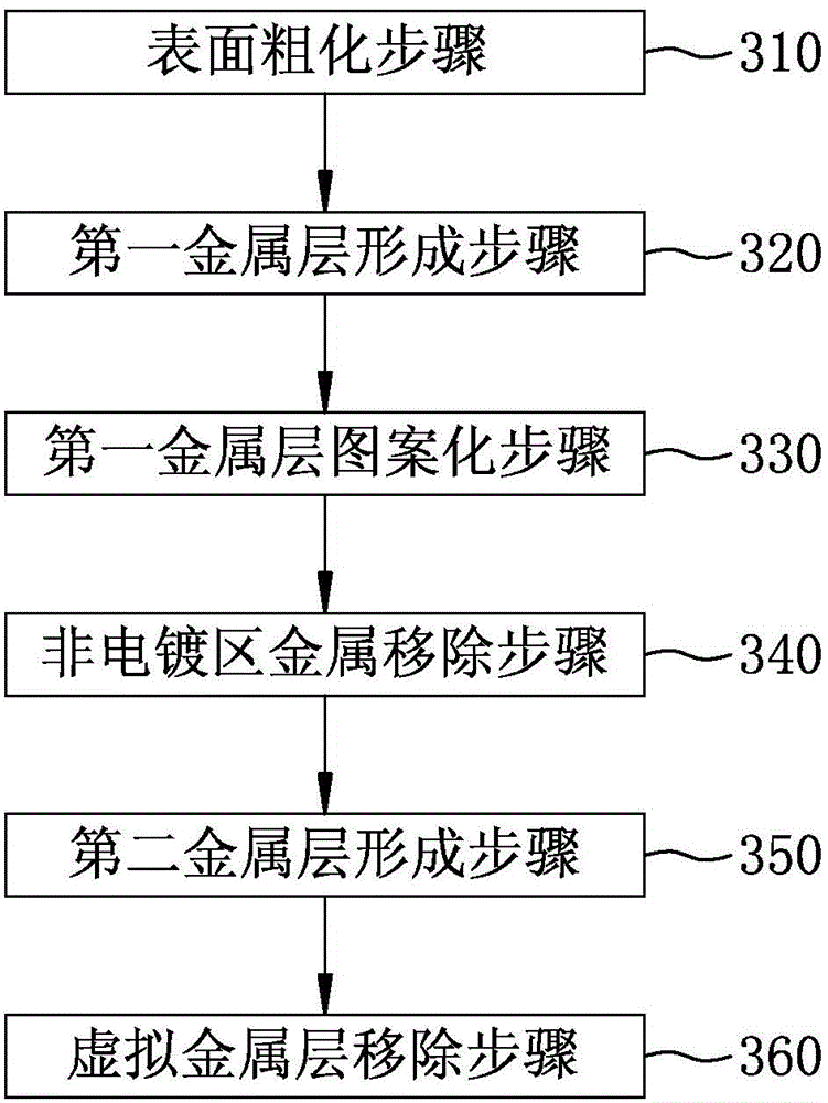
[0027] refer to figure 1 , an embodiment of the electroplating method with uniform metal coating thickness of the present invention, comprising the following steps:
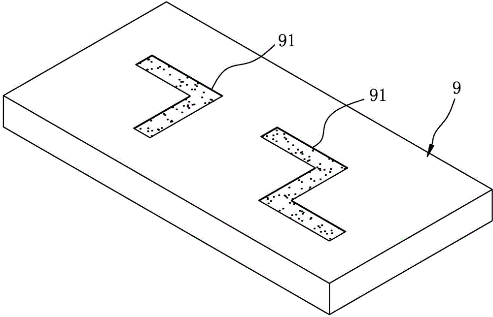
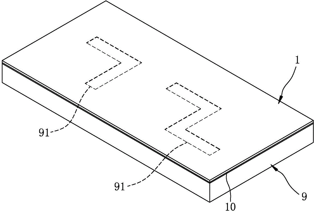
[0028] collocation reference figure 2 , a surface roughening step 310: according to the required electroplating pattern, laser processing is performed on a non-conductive substrate 9, so that most of the actual electroplating pattern areas formed by laser ablation are formed on the surface of the non-conductive substrate 9 91. The laser includes but not limited to infrared pulse laser and green pulse laser, the power of which can be between 6.0-13.0W, and the pulse frequency can be between 5.0-30.0kHz. The surface of each actual electroplating pattern area 91 has a microstructure, which can increase the roughness of the surface of the non-conductive substrate 9 and improve the adhesi...
PUM
 Abstract
Description
Claims
Application Information
 - R&D
- Intellectual Property
- Life Sciences
- Materials
- Tech Scout
- Unparalleled Data Quality
- Higher Quality Content
- 60% Fewer Hallucinations
Browse by: Latest US Patents, China's latest patents, Technical Efficacy Thesaurus, Application Domain, Technology Topic, Popular Technical Reports.
© 2025 PatSnap. All rights reserved.Legal|Privacy policy|Modern Slavery Act Transparency Statement|Sitemap|About US| Contact US: help@patsnap.com