Check patentability & draft patents in minutes with Patsnap Eureka AI!

Printed circuit board and pad surface treatment method for mobile terminal

A technology for printed circuit boards and mobile terminals, applied in the secondary processing of printed circuits, printed circuit parts, electrical connection printed components, etc., can solve the problems of unfavorable finished product yield, long production cycle, high cost, etc., and it is easier to achieve the yield rate Controlling, reducing production cost and time, and simplifying the process

Active Publication Date: 2017-10-24
SHANGHAI CHUANGGONG COMM TECH
View PDF8 Cites 0 Cited by
  • Summary
  • Abstract
  • Description
  • Claims
  • Application Information

AI Technical Summary

Problems solved by technology

[0003] The technical problem to be solved by the present invention is to overcome the disadvantages of the existing technology, such as unfavorable product yield, high cost and long production cycle, and to provide a method for better control of yield, lower cost and shorter production cycle. Printed circuit board of mobile terminal and method for surface treatment of pads thereof

Method used


Image

  • Printed circuit board and pad surface treatment method for mobile terminal
  • Printed circuit board and pad surface treatment method for mobile terminal

Examples


Embodiment Construction

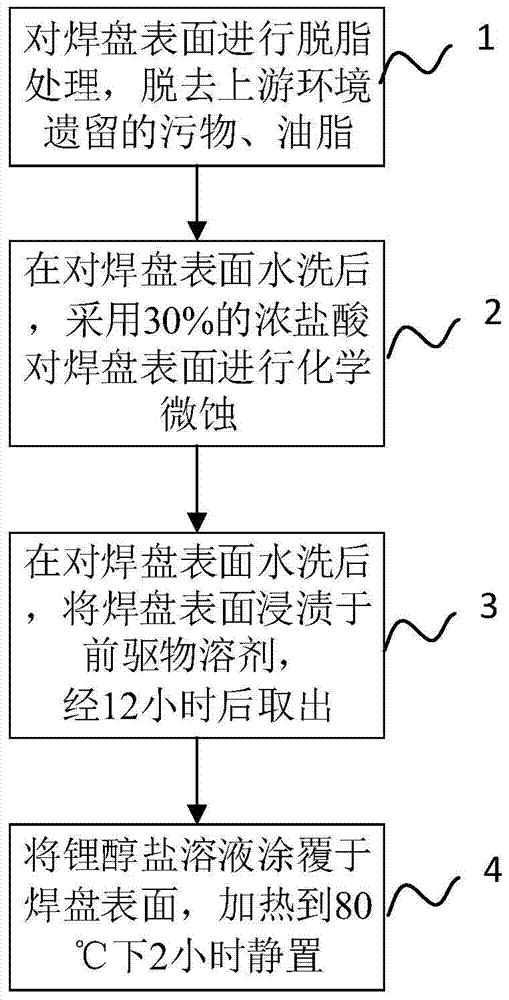
[0022] The present invention is further illustrated below by means of examples, but the present invention is not limited to the scope of the examples.

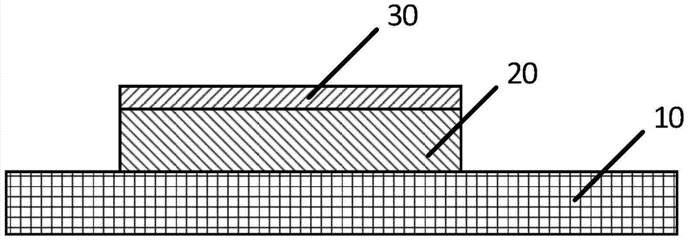
[0023] figure 1 It is a structural schematic diagram of a printed circuit board for a mobile terminal in this embodiment, as figure 1 As shown, the printed circuit board used in the mobile terminal involved in this embodiment includes a printed circuit board 10 and a plurality of solder pads 20, and an organic metal protective layer 30 is disposed on the solder pads.

[0024] The organometallic protective layer 30 is formed by polycondensation of metal alkoxide and organic precursor on the pad surface after alcoholysis. The thickness of the organometallic protective layer is 60-70nm.

[0025] The principle is to use the sol-gel method. The main reaction process is that the organic and inorganic precursors are dissolved in the co-solvent to form a uniform solution. The reactants produce alcoholysis reaction and then carry out...


PUM


Abstract

The invention discloses a printed circuit board for a mobile terminal, which includes a plurality of welding pads, and an organic metal protection layer is arranged on the welding pads. The present invention also provides a pad surface treatment method for mobile terminal printed circuit boards, which includes the following steps: S1, degreasing the pad surface; S2, chemical micro-etching the pad surface; S3 1. Immerse the surface of the pad in the precursor solvent for 8 to 24 hours and then take it out; S4. Apply the metal alkoxide solution to the surface of the pad; S5. Conduct electrical measurement on the printed circuit board. The organic metal protective layer that can conduct electricity is produced by the reaction of metal salt solution. While protecting the surface of the pad, the electrical measurement procedure is post-installed, which makes the yield rate easier to control, simplifies the process, and reduces production costs and time.

Description

technical field [0001] The invention relates to a mobile terminal, in particular to a printed circuit board for a mobile terminal and a method for treating the surface of a pad thereof. Background technique [0002] At present, on the PCB (printed circuit board) of mobile terminal equipment, the protective treatment of pads and exposed copper is based on the whole board chemical nickel gold process or chemical nickel gold combined with organic solder protection film (OSP, Organic Solderability Preservatives) process. host. The purpose of using the whole board of chemical nickel gold is to allow the pad and exposed copper to be fully protected against oxidation and wear (such as the surface protection of the keypad of the mobile phone), and to ensure solderability and sufficient conductivity of the metal contact surface, but In the PCB production process of this process, when encountering highly dense BGA (ball grid array structure PCB, Ball Grid Array) array pads, jump plat...

Claims


Application Information

Patent Timeline
Patent Type & Authority Patents(China)
IPC IPC(8): H05K1/02H05K1/11H05K3/22
Inventor 黄成树
Owner SHANGHAI CHUANGGONG COMM TECH
Features
  • R&D
  • Intellectual Property
  • Life Sciences
  • Materials
  • Tech Scout
  • Unparalleled Data Quality
  • Higher Quality Content
  • 60% Fewer Hallucinations
Learn More