Chip bonding film with cutting disk, semiconductor device, and manufacturing method for semiconductor device
A chip bonding and dicing chip technology, which is applied in semiconductor/solid-state device manufacturing, semiconductor devices, film/sheet-like adhesives, etc., can solve the problems of semiconductor wafer holding force reduction, fluidity reduction, peeling reduction, etc., Achieve the effect of suppressing cracks, preventing peeling, and not easy to break
- Summary
- Abstract
- Description
- Claims
- Application Information
AI Technical Summary
Problems solved by technology
Method used
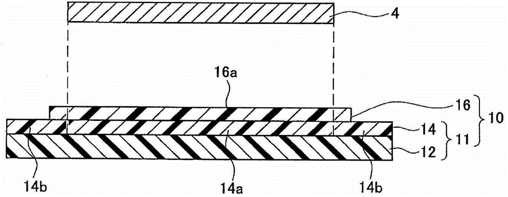
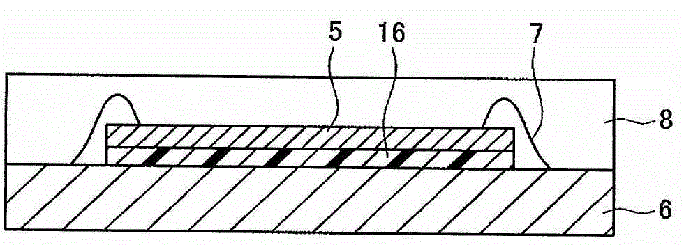
Image

Examples
Example Embodiment
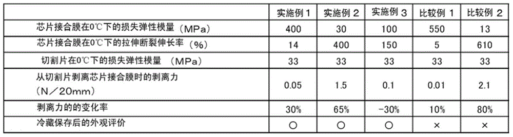
[0153] (Example 1)
[0154] The following (a) to (b) were dissolved in methyl ethyl ketone to obtain an adhesive composition solution having a concentration of 23% by weight.
[0155] (a) Acrylate copolymer with ethyl acrylate, butyl acrylate and acrylonitrile as main monomers (manufactured by Nagase Kasei Co., Ltd., trade name: SG-708-6, content of each main monomer: acrylic acid 51 wt% ethyl ester, 26 wt% butyl acrylate, 19 wt% acrylonitrile)
[0156] 97 copies
[0157] (b) Filler (manufactured by Admatechs, product name: SO-E1, average particle size: 0.25 μm)
[0158] 100 servings
[0159] This adhesive composition solution was applied to a release treated film (release liner) formed of a 38 μm thick polyethylene terephthalate film after silicone release treatment, and dried at 130°C 2 minute. Thus, a die-bonding film A having a thickness of 20 μm was produced.
Example Embodiment
[0160] (Example 2)
[0161] The following (a) to (b) were dissolved in methyl ethyl ketone to obtain an adhesive composition solution having a concentration of 23% by weight.
[0162] (a) Acrylate copolymer with ethyl acrylate, butyl acrylate and acrylonitrile as main monomers (manufactured by Nagase Kasei Co., Ltd., trade name: SG-708-6, content of each main monomer: acrylic acid 51 wt% ethyl ester, 26 wt% butyl acrylate, 19 wt% acrylonitrile)
[0163] 83 copies
[0164] (b) Thermal crosslinking agent (liquid epoxy resin (softening point: below 0°C), manufactured by Mitsubishi Chemical Corporation, product name: JER828)
[0165] 12 servings
[0166] This adhesive composition solution was applied to a release treated film (release liner) formed of a 38 μm thick polyethylene terephthalate film after silicone release treatment, and dried at 130°C 2 minute. Thus, a die-bonding film B having a thickness of 20 μm was produced.
Example Embodiment
[0167] (Example 3)
[0168] The following (a) to (b) were dissolved in methyl ethyl ketone to obtain an adhesive composition solution having a concentration of 23% by weight.
[0169] (a) Acrylate copolymer with ethyl acrylate, butyl acrylate and acrylonitrile as main monomers (manufactured by Nagase Kasei Co., Ltd., trade name: SG-P3, content of each main monomer: ethyl acrylate 30% by weight, 39% by weight of butyl acrylate, 28% by weight of acrylonitrile)
[0170] 90 servings
[0171] (b) Thermal crosslinking agent (liquid phenol resin (softening point: below 0°C), manufactured by Meiwa Chemical Co., Ltd., product name: MEH-8000H)
[0172] 5 servings
[0173] This adhesive composition solution was applied to a release treated film (release liner) formed of a 38 μm thick polyethylene terephthalate film after silicone release treatment, and dried at 130°C 2 minute. Thus, a die-bonding film C having a thickness of 20 μm was produced.
PUM
| Property | Measurement | Unit |
|---|---|---|
| The average particle size | aaaaa | aaaaa |
| Softening point | aaaaa | aaaaa |
| Thickness | aaaaa | aaaaa |
Abstract
Description
Claims
Application Information
 - R&D Engineer
- R&D Manager
- IP Professional
- Industry Leading Data Capabilities
- Powerful AI technology
- Patent DNA Extraction
Browse by: Latest US Patents, China's latest patents, Technical Efficacy Thesaurus, Application Domain, Technology Topic.
© 2024 PatSnap. All rights reserved.Legal|Privacy policy|Modern Slavery Act Transparency Statement|Sitemap