Check patentability & draft patents in minutes with Patsnap Eureka AI!

Chip and method for manufacturing chip

A chip and transistor technology, applied in semiconductor/solid-state device manufacturing, electrical components, transistors, etc., can solve problems such as illegal sales and design leaks

Active Publication Date: 2018-06-29
INFINEON TECH AG
View PDF3 Cites 0 Cited by
  • Summary
  • Abstract
  • Description
  • Claims
  • Application Information

AI Technical Summary

Problems solved by technology

An attacker who successfully reverse-engineers an integrated circuit can manufacture and sell similar or cloned circuits and can illegally sell and distribute their designs

Method used


Image

  • Chip and method for manufacturing chip
  • Chip and method for manufacturing chip
  • Chip and method for manufacturing chip

Examples


Embodiment Construction

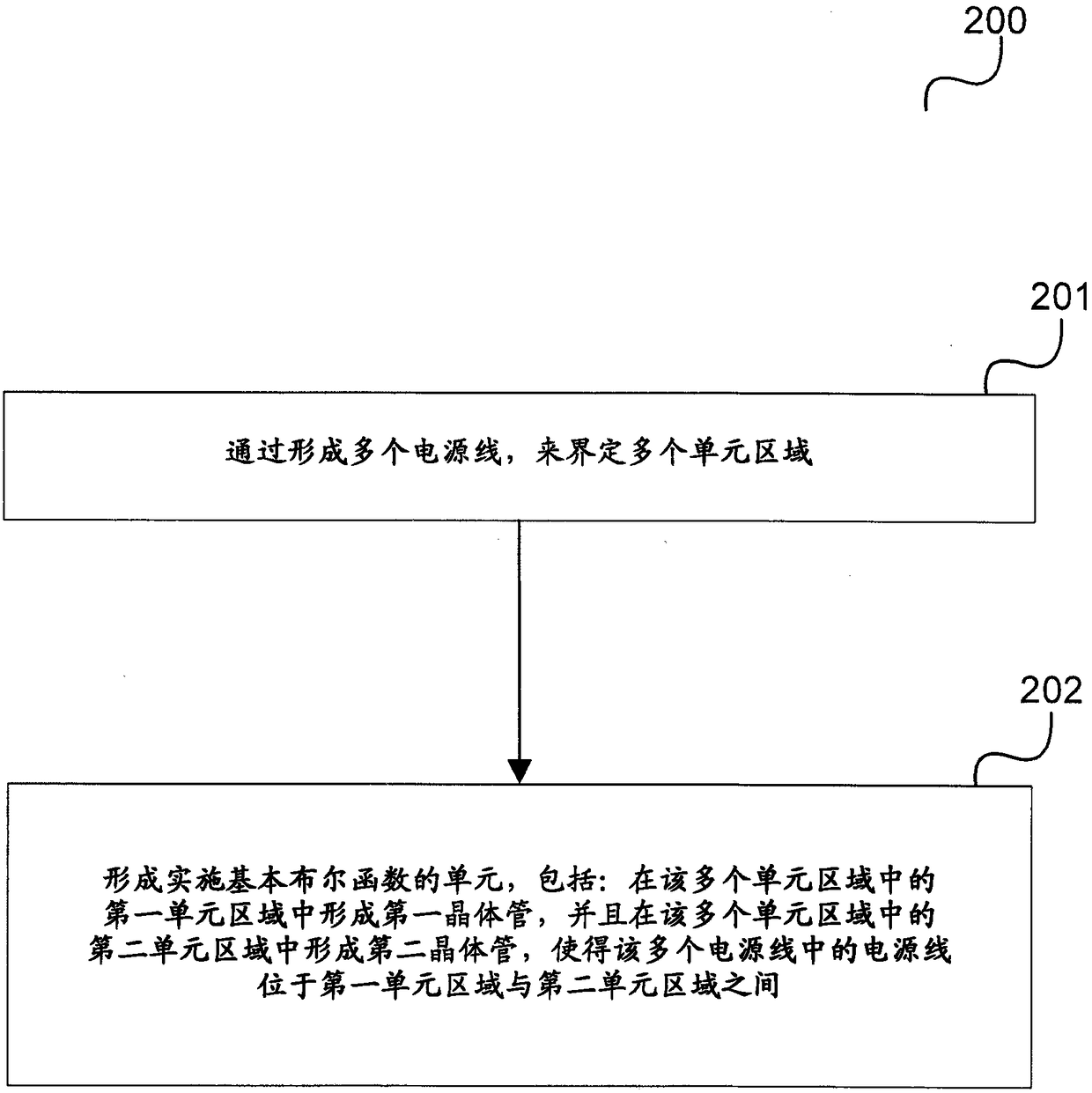
[0017] The following detailed description refers to the accompanying drawings, which show, by way of schematic illustration, specific details and aspects of the disclosure in which the invention may be practiced. Other aspects may be utilized and structural, logical, and electrical changes may be made without departing from the scope of the present invention. The various aspects of this disclosure need not be mutually exclusive, as some aspects of this disclosure can be combined with one or more other aspects of this disclosure to form new aspects.

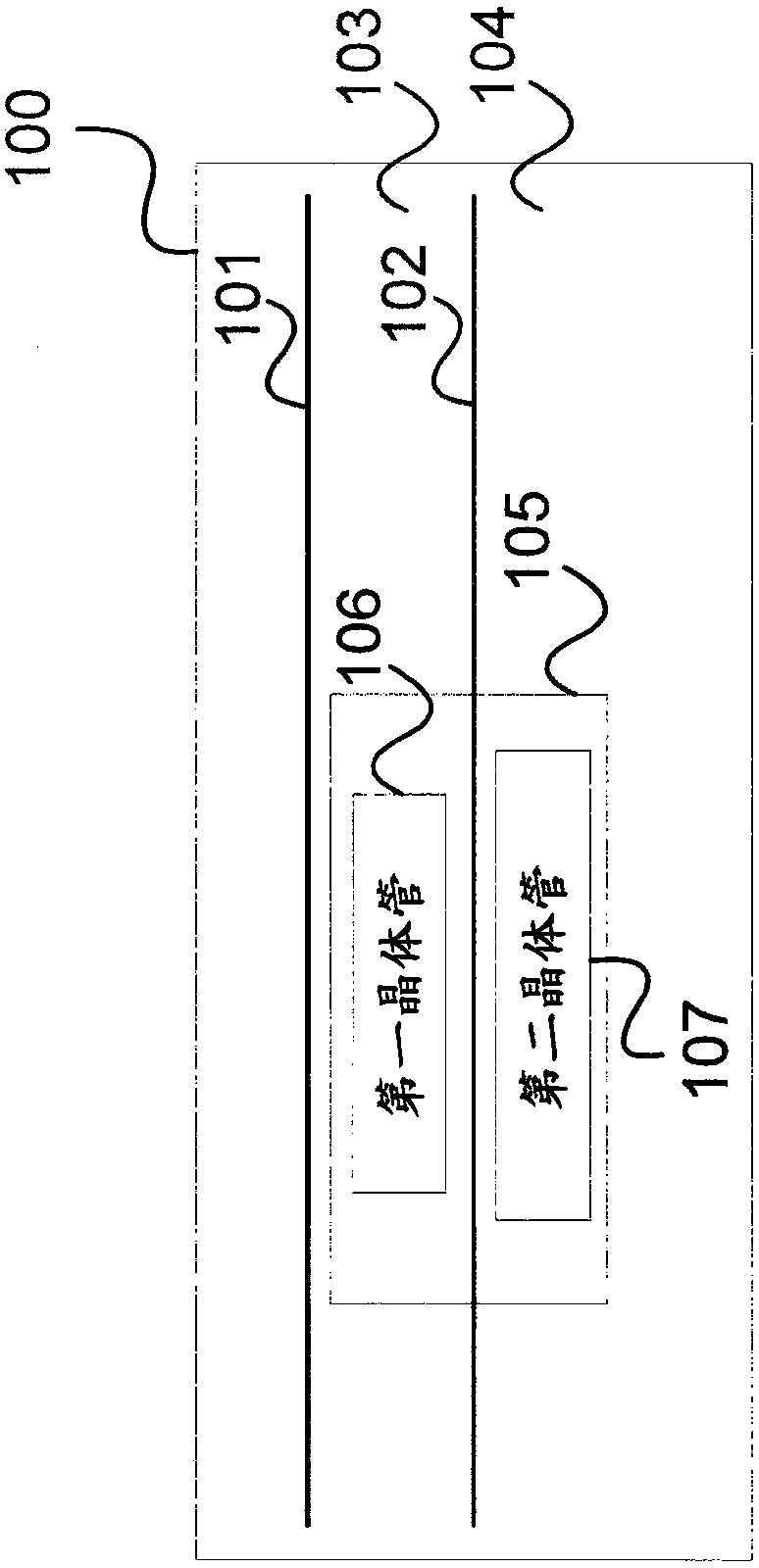
[0018] Reverse engineering can be thwarted by configuring a disguised circuit. However, these typically require process technology extensions, such as doping profile modifications, dummy contacts or vias, and / or suffer significantly increased area and power consumption. Therefore, these measures are usually too expensive for large-scale product manufacturing, for example in terms of license fees, silicon area, or energy consumpti...


PUM


Abstract

Various embodiments of the present invention relate to chips and methods for making chips. According to one embodiment, a chip is described that includes a plurality of power lines defining a plurality of cell regions, and a gate including a first transistor and a second transistor, wherein the first transistor is located in a first one of the plurality of cell regions cell region, and the second transistor is positioned in a second cell region of the plurality of cell regions, such that a power supply line of the plurality of power supply lines is located between the first cell region and the second cell region.

Description

technical field [0001] The present disclosure relates to chips and methods for manufacturing chips. Background technique [0002] Reverse engineering (RE) of integrated circuits (ICs) can be considered one of the most serious threats to the semiconductor industry because it can be misused by attackers to steal and / or pirate circuit designs. An attacker who successfully reverse-engineers an integrated circuit can manufacture and sell similar, or cloned, circuits, and can illegally sell and distribute their designs. [0003] There is therefore a need for concepts and techniques that hinder the reverse engineering of integrated circuits. Contents of the invention [0004] According to one embodiment, there is provided a chip comprising a plurality of power supply lines defining a plurality of cell areas and a gate comprising a first transistor and a second transistor, wherein the first transistor is located in a first cell area of ​​the plurality of cell areas And the secon...

Claims


Application Information

Patent Timeline
Patent Type & Authority Patents(China)
IPC IPC(8): H01L27/02H01L21/82
CPCH01L27/0203H01L27/088H01L27/092H01L2924/0002H01L23/5286H01L23/57H03K19/215H03K19/17768H01L2924/00H01L27/0207H01L27/11807H01L23/576
Inventor T·屈尔孟德B·利普曼
Owner INFINEON TECH AG
Features
  • R&D
  • Intellectual Property
  • Life Sciences
  • Materials
  • Tech Scout
  • Unparalleled Data Quality
  • Higher Quality Content
  • 60% Fewer Hallucinations
Learn More