Array substrate, manufacturing method thereof, liquid crystal display panel and display device

A technology for array substrates and base substrates, applied in optics, instruments, electrical components, etc., can solve problems such as complex manufacturing processes, achieve the effects of simplifying manufacturing processes, increasing aperture ratio, and reducing one-time patterning process

Pending Publication Date: 2015-11-25
BOE TECH GRP CO LTD
View PDF10 Cites 11 Cited by
  • Summary
  • Abstract
  • Description
  • Claims
  • Application Information

AI Technical Summary

Problems solved by technology

[0004] In the manufacturing process of the above-mentioned array substrate, a total of six

Method used


Image

  • Array substrate, manufacturing method thereof, liquid crystal display panel and display device
  • Array substrate, manufacturing method thereof, liquid crystal display panel and display device
  • Array substrate, manufacturing method thereof, liquid crystal display panel and display device

Examples


Example Embodiment

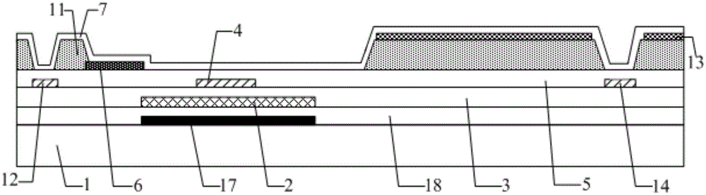
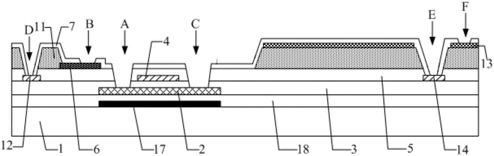
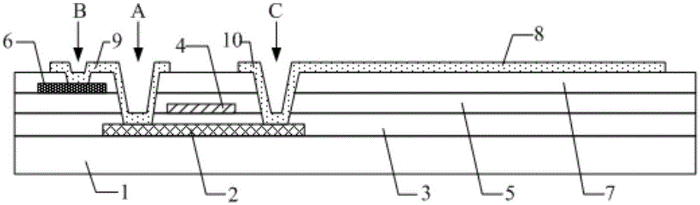
[0101] Example 1: Such as figure 2 The manufacturing method of the array substrate shown, such as Figure 7a-Figure 7m As shown, it can specifically include the following steps:

[0102] 1. Form a pattern including a light shielding layer 17 on the base substrate 1, such as Figure 7a Shown

[0103] 2. The buffer layer 18 is formed on the base substrate 1 with the pattern of the light shielding layer 17, such as Figure 7b Shown

[0104] 3. On the buffer layer 18, an amorphous silicon material is used to form the active layer film 19, and the active layer film 19 is subjected to an excimer laser annealing process, such as Figure 7c Shown

[0105] 4. Perform a patterning process on the active layer film 19 after the excimer laser annealing process to form a pattern including the active layer 2, such as Figure 7d Shown

[0106] 5. A gate insulating layer 3 is formed on the base substrate 1 on which the pattern of the active layer 2 is formed, such as Figure 7e Shown

[0107] 6. Form a ...


PUM


Abstract

The invention discloses an array substrate, a manufacturing method thereof, a liquid crystal display panel and a display device. According to the manufacturing method of the array substrate, after a first insulating layer is formed and before a source electrode is formed, it is not needed to form through holes which electrically connect the source electrode with an active layer through the composition process, but after a second insulating layer is formed and before a pixel electrode is formed, the composition process is conducted for forming a first through hole, a second through hole and a third through hole, the source electrode and the active layer are exposed, a first connecting portion is utilized for electrically connecting the source electrode with the active layer, wherein the first connecting portion and the pixel electrode are arranged on the same layer and insulated from each other, a second connecting portion is utilized as a drain electrode, wherein the second connecting portion and the pixel electrode are arranged on the same layer and electrically connected, and the second connecting portion is electrically connected with the active layer through the third through hole. Therefore, compared with manufacturing methods of existing array substrates, the composition process can be decreased by one time, and the array substrate manufacturing process can be simplified; in addition, the arrangement of the drain electrode can be omitted, thereby the aperture ratio of the array substrate can be raised.

Description

technical field [0001] The invention relates to the field of display technology, in particular to an array substrate, a manufacturing method thereof, a liquid crystal display panel and a display device. Background technique [0002] Among existing display devices, liquid crystal display devices (Liquid Crystal Display, LCD) have the advantages of low power consumption, high display quality, no electromagnetic radiation, and wide application range, and are currently more important display devices. [0003] An existing LCD array substrate generally includes: a base substrate, a thin film transistor and a pixel electrode located on the base substrate; wherein, the thin film transistor includes a gate, an active layer, a source and a drain. Thin-film transistors are divided into two types: top-gate type and bottom-gate type. Taking an array substrate with a top-gate type TFT as an example, the manufacturing process includes the following steps: first, a pattern of an active laye...

Claims


Application Information

Patent Timeline
IPC IPC(8): G02F1/1368G02F1/1333H01L27/12
Inventor 张斌舒适刘聖烈周婷婷曹占锋
Owner BOE TECH GRP CO LTD
Why Eureka
Try Eureka