

Array substrate and manufacturing method thereof, display apparatus
An array substrate and a substrate technology are applied in the fields of array substrates, their preparation, and display devices, which can solve the problems of small area and easy falling off of photoresist, and achieve the effect of large area and not easy to fall off.
- Summary
- Abstract
- Description
- Claims
- Application Information
AI Technical Summary
Problems solved by technology
Method used
Image


Examples
Embodiment 1
[0031] This embodiment provides a method for preparing an array substrate, including the following steps:
[0032] forming a semiconductor material layer on the substrate,
[0033] Coating photoresist on the semiconductor material layer,
[0034] Use a mask to expose and develop the photoresist, so that the first region retains the photoresist of the first thickness, and the second region retains the photoresist of the second thickness, wherein the first thickness is greater than the second thickness, and the first region retains the photoresist of the second thickness. is a region corresponding to the active region of the thin film transistor, and each first region is at least partially connected to the second region;
[0035] ashing to remove the photoresist in the second region, leaving at least part of the photoresist in the first region;
[0036] The substrate after the above steps is etched to remove the exposed semiconductor material layer to form the active region of...
Embodiment 2
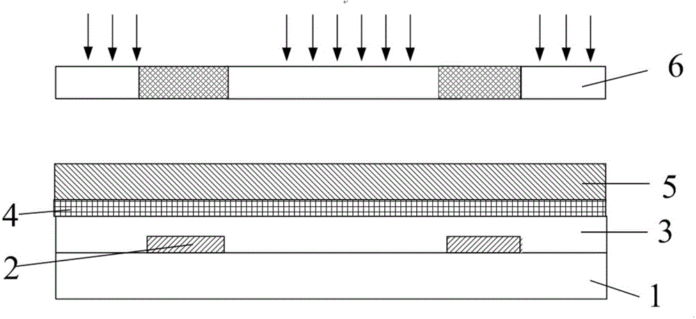
[0039] like Figure 3-5 As shown, this embodiment provides a method for preparing an array substrate, including the following steps:
[0040] S01 , forming a semiconductor material layer 4 on the substrate 1 .
[0041] The semiconductor material layer 4 is preferably a polysilicon layer.
[0042] Preferably, a step of cleaning the substrate 1 is also included between forming the semiconductor material layer on the substrate 1 and coating the photoresist 5 .
[0043] That is to say, in the prior art, there should be a step of cleaning the substrate 1 before coating the photoresist, but after cleaning the substrate 1, the photoresist 5 is coated, and the adhesion of the photoresist 5 is even worse. The photoresist 5 is more likely to fall off, and the step of cleaning the substrate 1 has to be abandoned. Due to the adoption of the semi-transparent exposure method, the contact area between the photoresist 5 and the substrate 1 after development is increased, even if the substr...
Embodiment 3
[0057] This embodiment provides an array substrate, which is prepared by the method in Embodiment 2.
[0058] Obviously, many changes can be made to the specific implementation of the above-mentioned embodiments; for example: the specific areas and forms of the first region and the second region can be designed according to needs, or different masks can be replaced according to different needs to achieve a certain value The first thickness and the second thickness.
PUM
| Property | Measurement | Unit |
|---|---|---|
| thickness | aaaaa | aaaaa |
| thickness | aaaaa | aaaaa |
Abstract
Description
Claims
Application Information