Assembling method for optical module and optical module
An assembly method and optical module technology, applied in the coupling of optical waveguides, light guides, optics, etc., can solve the problems of reducing the accuracy of optical modules, the light cannot be injected into the optical fiber, and the propagation path deviates from the set path, etc., so as to improve the yield rate, The effect of improving assembly accuracy and reducing waste
- Summary
- Abstract
- Description
- Claims
- Application Information
AI Technical Summary
Problems solved by technology
Method used
Image

Examples
Embodiment 1
[0028] In view of the fact that in the prior art, the use of glue to bond the lens assembly and the circuit board will affect the installation accuracy of the lens assembly, this embodiment provides an optical module assembly method that can reduce the displacement of the lens assembly during the installation process. Thus, the mounting accuracy is improved.
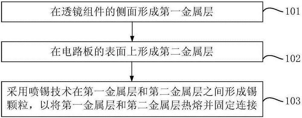
[0029] image 3 It is a flowchart of an optical module assembly method provided by an embodiment of the present invention. Such as image 3 As shown, the optical module assembly method provided in this embodiment includes:
[0030] Step 101, forming a first metal layer on the side of the lens assembly.
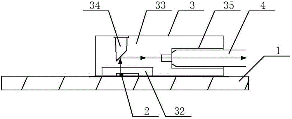
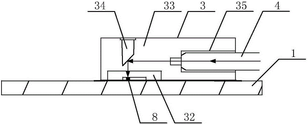
[0031] Figure 4 A schematic diagram of the structure of the first metal layer formed on the side of the lens assembly in the optical module provided by the embodiment of the present invention. Such as Figure 4 As shown, the bottom surface of the lens assembly 3 is the surface facing the circuit board 1 , and the ...
Embodiment 2
[0057] This embodiment provides an implementation of an optical module, which can be obtained by using the optical module assembly method provided in the first embodiment above. Specifically, the optical module includes: a circuit board 1 and a lens assembly 3, wherein the lens assembly 3 The bottom surface is in contact with the circuit board 1 . The side of the lens assembly 3 is provided with a first metal layer 31, and the surface of the circuit board 1 is provided with a second metal layer 11. When the lens assembly 3 is placed on the surface of the circuit board 1, the second metal layer 11 and the first metal layer 31 contacts. There are tin particles 7 between the first metal layer 31 and the second metal layer 11 for thermally melting and fixing the first metal layer 31 and the second metal layer 11 together.
[0058] Specifically, the bottom surface of the lens assembly 3 is a surface facing the circuit board 1 , and the side surface is a surface adjacent to the bot...
PUM
| Property | Measurement | Unit |
|---|---|---|
| diameter | aaaaa | aaaaa |
| thickness | aaaaa | aaaaa |
| diameter | aaaaa | aaaaa |
Abstract
Description
Claims
Application Information
 - R&D
- Intellectual Property
- Life Sciences
- Materials
- Tech Scout
- Unparalleled Data Quality
- Higher Quality Content
- 60% Fewer Hallucinations
Browse by: Latest US Patents, China's latest patents, Technical Efficacy Thesaurus, Application Domain, Technology Topic, Popular Technical Reports.
© 2025 PatSnap. All rights reserved.Legal|Privacy policy|Modern Slavery Act Transparency Statement|Sitemap|About US| Contact US: help@patsnap.com