A power module structure capable of improving welding quality

A power module and welding quality technology, applied in the direction of electrical components, electrical solid devices, circuits, etc., can solve problems such as short circuit failure, component mounting tilt, uneven solder coating thickness, etc., to prevent hot spots and cracks , prevent drift and tilt, and improve the effect of long-term reliability

Active Publication Date: 2016-01-27
NANJING HIGHSEMI ELECTRIC POWER SCI & TECH CO LTD
View PDF6 Cites 10 Cited by
  • Summary
  • Abstract
  • Description
  • Claims
  • Application Information

AI Technical Summary

Problems solved by technology

Due to process limitations, this process is prone to problems such as uneven solder coating thickness and component mounting tilt, which in turn will cause tilt or offset of the DBC substrate and power chip during the reflow soldering process. See figure 2
In addition, the uneven thickness of the first solder layer 6 and the second solder layer 2 will increase the stress suffered by the power chip by 2.2 times during the power cycle and temperature cycle [1] , the creep strain in the solder layer increases significantly [2] , affecting the long-term ser

Method used


Image

  • A power module structure capable of improving welding quality
  • A power module structure capable of improving welding quality
  • A power module structure capable of improving welding quality

Examples


Example Embodiment

[0027] The present invention will be further described in detail below in conjunction with the accompanying drawings.

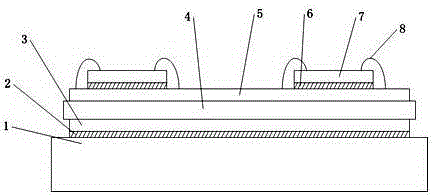
[0028] see figure 1 A typical power module in the prior art mainly includes a bottom plate 1, a DBC substrate 4, and a power chip 7. The upper and lower surfaces of the DBC substrate 4 are covered with an upper copper layer 5 and a lower copper layer 3, respectively. The power chip 7 is soldered to the upper copper layer 5 through the second solder layer 6, and the lower copper layer 3 is soldered to the bottom plate 1 through the first solder layer 2. The power chip 7 is bonded to the upper copper layer 5 by using a wire 8.

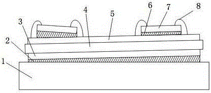
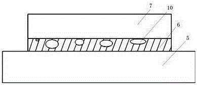
[0029] Figure 4~5 It is a schematic diagram of a specific structure of the power module of the present invention. Compared with a typical power module, the present invention has the following improvements: the upper surface of the base plate 1 is etched with a chamfered first recess that matches the first solder layer 2. The groove 11 is ...


PUM


Abstract

The invention provides a power module structure capable of improving welding quality. The power module structure comprises a bottom board, DBC substrates and power chips. The upper surface and the lower surface of each DBC substrate are covered with an upper copper layer and a lower copper layer respectively. The power chips are welded to the upper copper layers through second solder layers. The lower copper layers are welded to the bottom board through first solder layers. The power chips and the upper copper layers are bonded via leads. The upper surface of the bottom board is provided with etched first grooves with chamfers, which match the first solder layers. The first solder layers are applied in the first grooves. The upper surfaces of the upper copper layers are provided with etched second grooves with chamfers, which match the second solder layers. The second solder layers are applied in the second grooves. The structure can prevent unevenness of the thickness of the solder layers and overflow of solder, reduce cavities of the solder layers, and further improve the welding quality of the power module and improve the thermal property and the long-term reliability of the power module.

Description

technical field [0001] The invention belongs to the technical field of semiconductor chip packaging, in particular to a power module structure that can improve welding quality. Background technique [0002] At present, the interconnection process of power modules at home and abroad mainly adopts welding method, see figure 1 . In this packaging structure, the power chip 7 is reflow soldered to the upper copper layer 5 of the DBC substrate (copper-clad ceramic substrate) 4 through the first solder layer 6, and the DBC substrate 4 after welding the power chip is then reflowed through the second solder layer 2 Soldering on the base plate 1; or two reflow soldering processes are completed simultaneously. The DBC substrate is usually a sandwich structure, such as figure 1 Among them, its upper and lower surfaces are respectively covered with an upper copper layer 5 and a lower copper layer 3; the bottom plate 1 is usually made of high thermal and electrical conductivity materia...

Claims


Application Information

Patent Timeline
IPC IPC(8): H01L23/13H01L23/498
CPCH01L2224/32225H01L2224/48091H01L2224/48227H01L2224/73265H01L2924/00014H01L2924/00
Inventor 刘胜王淼操徐玲周洋
Owner NANJING HIGHSEMI ELECTRIC POWER SCI & TECH CO LTD
Why Eureka
Try Eureka