Check patentability & draft patents in minutes with Patsnap Eureka AI!

Power conversion device and elevator using the power conversion device

A power conversion device and circuit technology, applied in the direction of irreversible DC power input conversion to AC power output, electrical components, AC motor control, etc., can solve the problems of promoting current imbalance and shortening the life of semiconductor switching elements, etc., to achieve Suppresses the effect of lifespan shortening

Active Publication Date: 2018-04-10
HITACHI LTD
View PDF8 Cites 0 Cited by
  • Summary
  • Abstract
  • Description
  • Claims
  • Application Information

AI Technical Summary

Problems solved by technology

In this case, as already described, when a current imbalance occurs among a plurality of semiconductor switching elements, the current imbalance will be promoted, and the following problems will arise. A semiconductor switching element, therefore shortening the life of the semiconductor switching element
[0015] In addition, the IGBT has been described as an example in the description so far, but since the same source loop as the emitter loop exists in a MOSFET, etc., the loop path (emitter loop) on the drive circuit side road or source loop) will create the same problem

Method used


Image

  • Power conversion device and elevator using the power conversion device
  • Power conversion device and elevator using the power conversion device
  • Power conversion device and elevator using the power conversion device

Examples


Embodiment 1

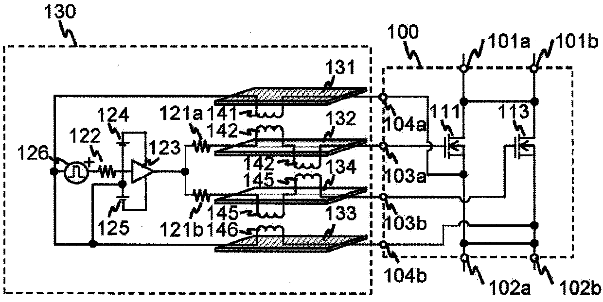
[0036] figure 1 It is a schematic diagram of the parallel circuit and the driving circuit of the first embodiment of the present invention. figure 1 the basic structure of Figure 13 as well as Figure 14 same, but in Figure 13 as well as Figure 14 IGBT is taken as an example as a semiconductor switching element in the description. In contrast, in figure 1 An example using a Metal-Oxide-Semiconductor Field Effect Transistor (MOSFET) is shown in . Hereafter, description will be made taking MOSFET as an example as a semiconductor switching element. For example, MOSFETs using silicon carbide (SiC) devices that can increase switching speed can be used. In addition, in the case of a MOSFET, since it has a built-in diode structure between the drain and the source, it is possible to omit an external anti-parallel connection diode necessary when using an IGBT, thereby omitting an external anti-parallel diode . exist figure 1 Here, only the semiconductor switching elements 1...

Embodiment 21

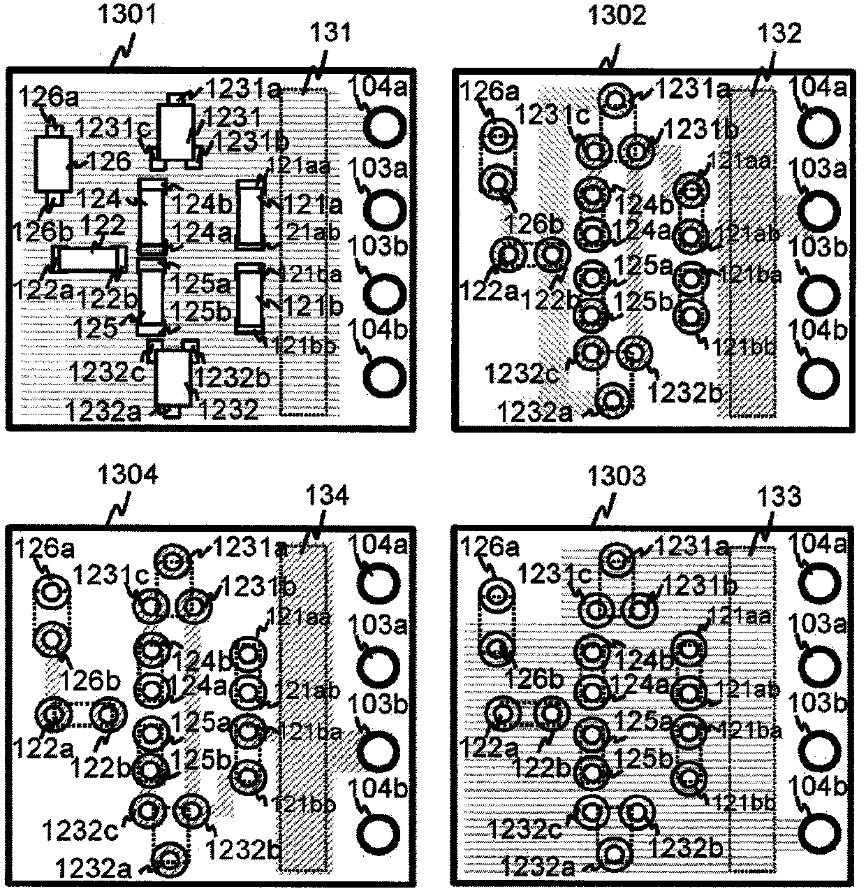
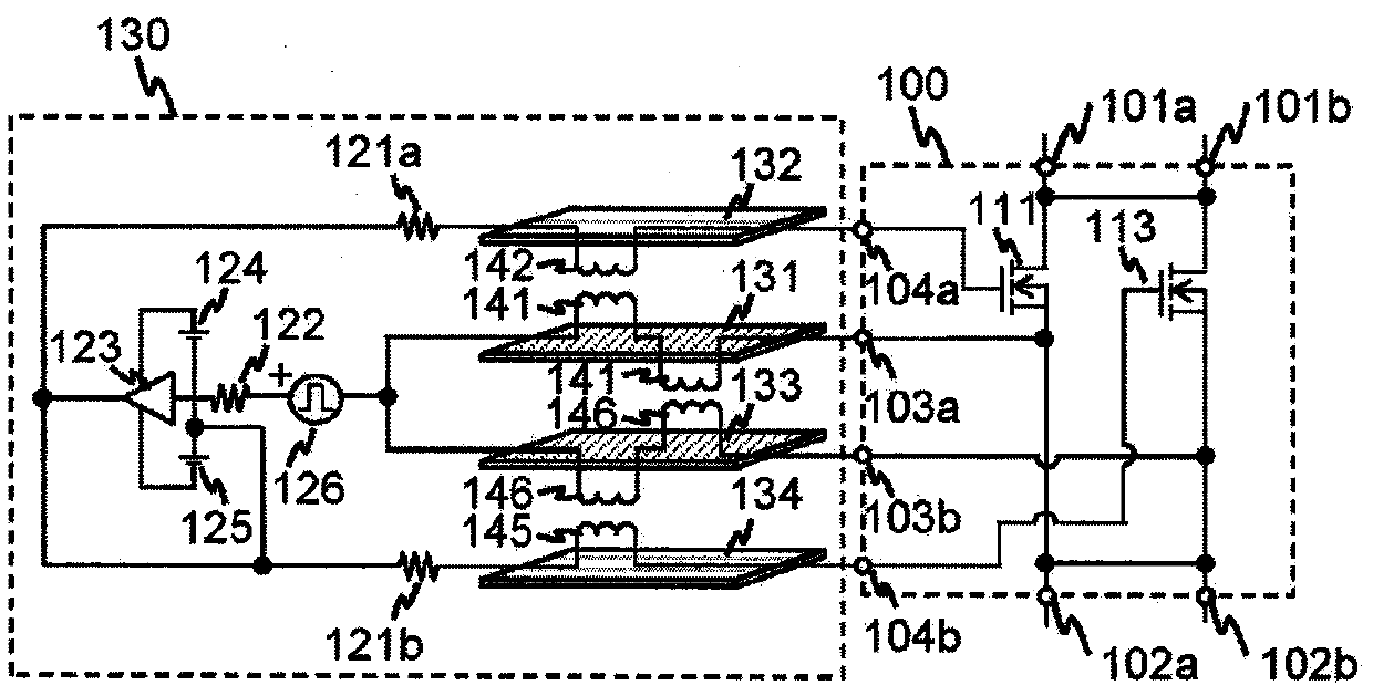
[0075] Figure 9 It is a schematic diagram of the parallel circuit and the driving circuit of the second embodiment of the present invention. The second embodiment differs from the first embodiment in that the sensing source layers and gate layers are alternately arranged. Specifically, in the multilayer substrate, the sensing source layer 1301 , the gate layer 1302 , the sensing source layer 1303 , and the gate layer 1304 are arranged in sequence.

[0076] In the second embodiment, although the interlayer distance between the sensing source layer 1301 and the sensing source layer 1303 is shorter than that of the first embodiment, since the gate layer 1302 is sandwiched between the sensing source layer 1301 and the sensing source layer 1303 to maintain an interlayer distance, so although the effect is smaller than that of the first embodiment, the same effect can be obtained.

Embodiment 31

[0078] Figure 10 It is a schematic diagram of the parallel circuit and the driving circuit of the third embodiment of the present invention. In the third embodiment, the difference from the second embodiment is that the number of parallel circuits 100 connected in parallel is three.

[0079] To this end, a semiconductor switching element 115 connected in parallel to the semiconductor switching elements 111 and 113 is added. 101c, 102c, 103c, and 104c are drain terminals connected to the drain, source, gate, and source of the semiconductor switching element 115, respectively. terminal, source terminal, gate terminal, sense source terminal.

[0080] In addition, the driving circuit 130 has a multilayer substrate having 6 layers, in addition to the sensing source layer and the gate layer of the semiconductor switching elements 111 and 113, and also has a sensing source layer 1305, which is a conductive layer with the same potential as the source (sensing source) of the semicon...


PUM


Abstract

The invention provides a power conversion device and an elevator using the power conversion device. In a condition that a drive circuit with a multilayer substrate enables simultaneous on-off of a plurality of semiconductor switch elements, through making flowing of currents towards a loop path of a drive circuit side, fostering of current imbalance between the plurality of the semiconductor switch elements is suppressed. A plurality of conducting layers of the multilayer substrate of the drive circuit which enables simultaneous on-off of the plurality of semiconductor switch elements which are in parallel connection is provided at different positions in a thickness direction with a first conducting layer having the same potential as a second terminal (a source electrode or an emitter electrode) of a first semiconductor switch element, a second conducting layers having the same potential as a second terminal of a second semiconductor switch element and a third conducting layer having the same potential as a first terminal (grid electrode) of a first semiconductor switch element. The third conducting layer is clamped between the first conducting layer and the second conducting layer.

Description

technical field [0001] The present invention relates to a power conversion device and an elevator using the power conversion device. Background technique [0002] At present, in the variable-speed driving of elevators and the like, it is common to convert electric power into variable-frequency alternating current via an inverter to drive a motor. [0003] Figure 13 This is a conventional example of a power conversion device. exist Figure 13 A schematic configuration of an inverter is shown as an example of a generally used power conversion device. exist Figure 13 Among them, 10 , 30 , and 50 represent one phase of an inverter circuit, which converts the DC power smoothed by the capacitor 11 into AC with variable frequency, and drives the motor 12 . 111, 211, 311, 411, 511, and 611 denote semiconductor switching elements, and an example using an IGBT is shown here. 112 , 212 , 312 , 412 , 512 , and 612 are diodes, which are respectively connected in antiparallel to the ...

Claims


Application Information

Patent Timeline
Patent Type & Authority Patents(China)
IPC IPC(8): H02M7/48H02P27/06
Inventor 加藤香森和久大沼直人薮内达志松本洋平迫田友治
Owner HITACHI LTD
Features
  • R&D
  • Intellectual Property
  • Life Sciences
  • Materials
  • Tech Scout
  • Unparalleled Data Quality
  • Higher Quality Content
  • 60% Fewer Hallucinations
Learn More