Production method of orientation layer and production method of display substrate
A manufacturing method and a display substrate technology, which are applied in optics, instruments, nonlinear optics, etc., can solve problems such as the inability to form an alignment layer, the inability of a transfer roller to transfer an alignment liquid, and the poor display effect of a liquid crystal display device. Show the effect of the effect
- Summary
- Abstract
- Description
- Claims
- Application Information
AI Technical Summary
Problems solved by technology
Method used
Image

Examples
Embodiment 1
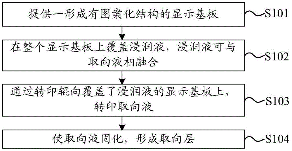
[0020] Embodiments of the present invention provide a method for fabricating an alignment layer, such as figure 1 Shown, the preparation method of this alignment layer comprises:
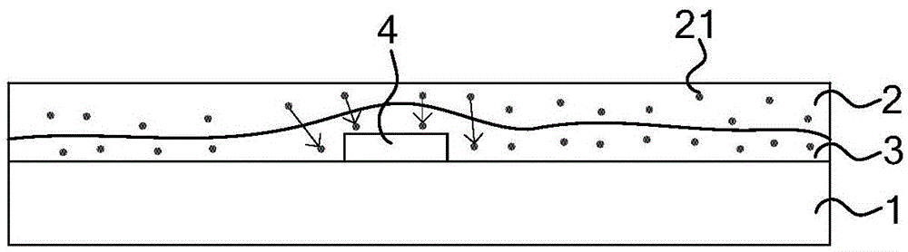
[0021] Step S101 , providing a display substrate formed with a patterned structure. Exemplarily, the display substrate may be an array substrate or a color filter substrate. When the display substrate is an array substrate, the display substrate includes a base substrate, a thin film transistor disposed on the base substrate, a passivation layer covering the thin film transistor, and a pixel electrode located on the passivation layer. The patterned structure is a pixel electrode; when the display substrate is a color filter substrate, the display substrate includes a base substrate, a black matrix and a color-resist layer arranged on the base substrate, and a common electrode located on the black matrix and the color-resist layer , at this time, the patterned structure on the display substrate is ...
Embodiment 2
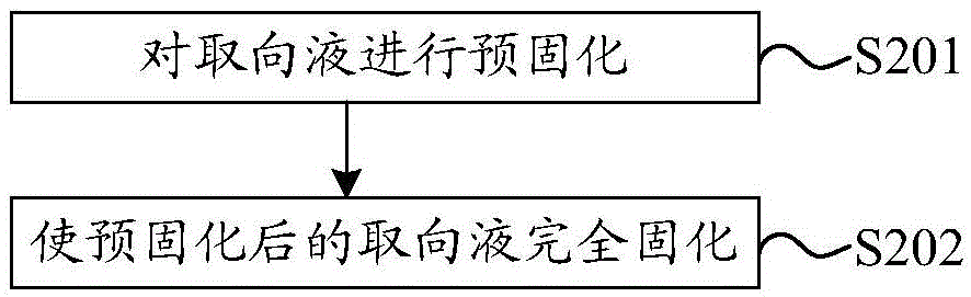
[0037] An embodiment of the present invention provides a method for manufacturing a display substrate. The method for manufacturing a display substrate includes using the method for manufacturing an alignment layer as described in Embodiment 1 to manufacture an alignment layer on a display substrate.
[0038] Since the manufacturing method of the display substrate provided by the embodiment of the present invention includes using the method for manufacturing the alignment layer described in the first embodiment to make an alignment layer on the display substrate, the method for manufacturing the display substrate has the same characteristics as that described in the first embodiment. The beneficial effect is the same as the manufacturing method of the above-mentioned alignment layer, and will not be repeated here.
[0039] Specifically, when the display substrate is an array substrate, the manufacturing method of the display substrate may further include the following steps: fi...
PUM
| Property | Measurement | Unit |
|---|---|---|
| percent by mass | aaaaa | aaaaa |
Abstract
Description
Claims
Application Information
 - R&D
- Intellectual Property
- Life Sciences
- Materials
- Tech Scout
- Unparalleled Data Quality
- Higher Quality Content
- 60% Fewer Hallucinations
Browse by: Latest US Patents, China's latest patents, Technical Efficacy Thesaurus, Application Domain, Technology Topic, Popular Technical Reports.
© 2025 PatSnap. All rights reserved.Legal|Privacy policy|Modern Slavery Act Transparency Statement|Sitemap|About US| Contact US: help@patsnap.com