Check patentability & draft patents in minutes with Patsnap Eureka AI!

ADC built-in self-test circuit and test method in system on chip

A built-in self-test, system-on-chip technology, applied in the field of analog/mixed-signal integrated circuit testing, to achieve the effects of saving storage resources, improving computing accuracy, and reducing computing complexity

Active Publication Date: 2018-09-11
INST OF MICROELECTRONICS CHINESE ACAD OF SCI
View PDF5 Cites 0 Cited by
  • Summary
  • Abstract
  • Description
  • Claims
  • Application Information

AI Technical Summary

Problems solved by technology

[0007] The present invention provides an ADC built-in self-test circuit and test method in an on-chip system to solve the problem in the prior art that the performance analysis can only be completed under the condition that there is a DSP on the chip

Method used


Image

  • ADC built-in self-test circuit and test method in system on chip
  • ADC built-in self-test circuit and test method in system on chip
  • ADC built-in self-test circuit and test method in system on chip

Examples


Embodiment Construction

[0066] In order to enable those skilled in the art to better understand the solutions of the embodiments of the present invention, the embodiments of the present invention will be further described in detail below in conjunction with the drawings and implementations.

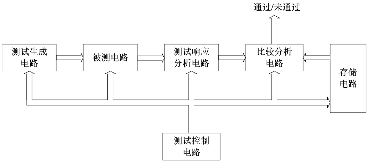
[0067] Such as figure 1 As shown, it is a schematic structural diagram of the ADC built-in self-test circuit in the system on chip of the embodiment of the present invention.

[0068] The circuit 100 includes: a control module 11 , a signal processing module 12 and a testing module 13 . in:

[0069] The control module 11 is configured to trigger the signal processing module 12 and the test module 13 to start working after the response signal output by the ADC to be tested is stable after the excitation signal is applied;

[0070] The signal processing module 12 is configured to sample the response signal, perform FFT transformation on the sampled value real sequence obtained by sampling, and obtain the spectru...


PUM


Abstract

The present invention discloses a built-in self-test (BIST) circuit and a testing method of an analog to digital converter (ADC) in a system on chip (SoC). The circuit comprises a control module, a signal processing module and a testing module. The control module is used for triggering the signal processing module and the testing module to start working when a response signal output by an under-test ADC after a drive signal is applied to the under-test ADC becomes stable; the signal processing module is used for sampling the response signal and carrying out fast fourier transformation (FFT) on a sampled sampling value real sequence, thus to obtain spectrum signal data of the response signal; and the testing module is used for calculating dynamic parameters of the response signal according to the spectrum signal data of the response signal. With adoption of the circuit and the method, a BIST of an on-chip ADC can be realized without any dependence on on-chip digital signal processors (DSP).

Description

technical field [0001] The invention relates to the field of analog / mixed-signal integrated circuit testing, in particular to an ADC built-in self-testing circuit and a testing method in an on-chip system. Background technique [0002] Integrated circuit technology has developed to the stage of SoC (system on chip), and testing is one of the key technologies of SoC. SoC test structure and test method become the main research field of testability design recently. In addition to integrating a large number of digital circuit IP (intellectual property) cores, SoC also integrates analog mixed-signal IP cores. For analog hybrid circuits, since there is no widely accepted fault model and mature testability design tool support like digital integrated circuits, most of the tests of analog hybrid circuits are based on functional and parameter tests. Studying the test structure and self-test method of analog hybrid circuits in SoC is an urgent problem to be considered and solved in S...

Claims


Application Information

Patent Timeline
Patent Type & Authority Patents(China)
IPC IPC(8): H03M1/10
CPCH03M1/1095
Inventor 柳臻朝陈岚冯燕王东
Owner INST OF MICROELECTRONICS CHINESE ACAD OF SCI
Features
  • R&D
  • Intellectual Property
  • Life Sciences
  • Materials
  • Tech Scout
  • Unparalleled Data Quality
  • Higher Quality Content
  • 60% Fewer Hallucinations
Learn More