Multi-layer flexible circuit board and preparation method thereof
A flexible circuit board and flexible substrate technology, applied in multilayer circuit manufacturing, printed circuit manufacturing, printed circuit, etc., can solve problems such as wrinkles, defects, and poor wiring, and reduce corrosion and oxidation, reduce costs, and improve The effect of yield
- Summary
- Abstract
- Description
- Claims
- Application Information
AI Technical Summary
Problems solved by technology
Method used
Image

Examples
Embodiment 1
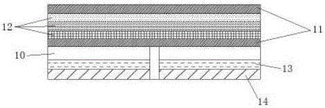
[0026] This embodiment provides a multi-layer flexible circuit board, which includes a flexible substrate 10 and a first metal layer 13 and a second metal layer 14 arranged in sequence on the back of the flexible substrate; five conductive layers 11 and 12; through holes 20 are provided in the flexible substrate, and the through holes are formed by punching holes along the thickness direction of the back surface of the substrate; the conductive layer on the upper layer is formed by hot melt adhesive coated on the surface of the upper conductive layer The layer is connected with the conductive layer of the lower layer; the conductive layer of the lowermost layer is connected to the flexible substrate through the hot melt adhesive layer coated on the surface of the conductive layer of the lowermost layer; the conductive layer except the uppermost layer is printed with a circuit layer .
[0027] The circuit layer and the hot-melt adhesive layer are respectively disposed on the su...
Embodiment 2
[0041] This embodiment provides a multi-layer flexible circuit board, the multi-layer flexible circuit board includes a flexible substrate, a first metal layer and a second metal layer arranged in sequence on the back of the flexible substrate; three conductive layers are arranged on the front of the flexible substrate; The flexible substrate is provided with through holes, and the through holes are formed by drilling through holes along the thickness direction of the back surface of the substrate; the conductive layer on the upper layer is connected to the conductive layer on the lower layer through a hot melt adhesive layer coated on the surface of the upper conductive layer. ; The lowermost conductive layer is connected with the flexible substrate via a hot melt adhesive layer coated on the surface of the lowermost conductive layer; a circuit layer is printed on the conductive layers except the uppermost layer.
[0042] The circuit layer and the hot-melt adhesive layer are r...
Embodiment 3
[0056] This embodiment provides a multi-layer flexible circuit board, the multi-layer flexible circuit board includes a flexible substrate, a first metal layer and a second metal layer arranged in sequence on the back of the flexible substrate; four conductive layers are arranged on the front of the flexible substrate There are through holes in the flexible substrate, and the through holes are formed by punching holes along the thickness direction of the back of the substrate; connection; the lowermost conductive layer is connected with the flexible substrate through a hot melt adhesive layer coated on the surface of the lowermost conductive layer; a circuit layer is printed on the conductive layers except the uppermost layer.
[0057] The circuit layer and the hot-melt adhesive layer are respectively arranged on the surfaces of both sides of the conductive layer; the thickness of the hot-melt adhesive layer is 0.6 mm, and the thickness of the circuit layer is 0.3 mm.
[0058]...
PUM
| Property | Measurement | Unit |
|---|---|---|
| Thickness | aaaaa | aaaaa |
| Thickness | aaaaa | aaaaa |
| Thickness | aaaaa | aaaaa |
Abstract
Description
Claims
Application Information
 - R&D Engineer
- R&D Manager
- IP Professional
- Industry Leading Data Capabilities
- Powerful AI technology
- Patent DNA Extraction
Browse by: Latest US Patents, China's latest patents, Technical Efficacy Thesaurus, Application Domain, Technology Topic.
© 2024 PatSnap. All rights reserved.Legal|Privacy policy|Modern Slavery Act Transparency Statement|Sitemap