A Phase Plate for Phase Contrast Microscopy
A phase contrast microscope and phase plate technology, applied in the field of phase plates, can solve the problems of long production process flow, difficult to guarantee coating accuracy, limited processing efficiency, etc., to achieve improved imaging effect, shortened coating process flow, and reduced light source energy attenuation. Effect
- Summary
- Abstract
- Description
- Claims
- Application Information
AI Technical Summary
Problems solved by technology
Method used
Image

Examples
Embodiment 1
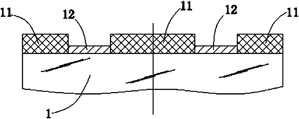
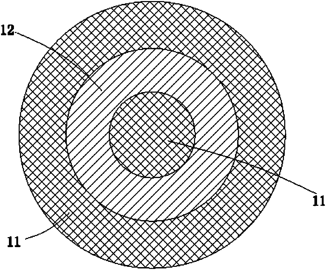
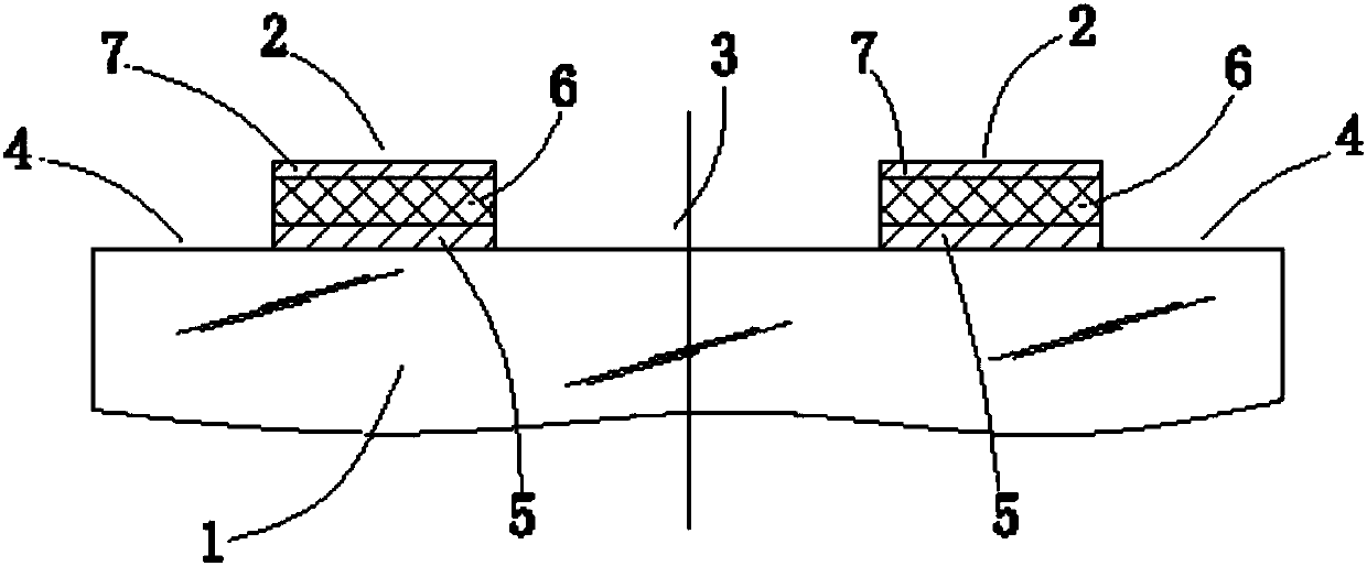
[0032] The glass substrate 1 is selected as an N-BK7 substrate. The bottom layer 5 and surface layer 7 of the annular thin film layer 2 are metal Cr film layers, the physical thickness of the bottom layer 5 of the annular thin film layer 2 is 8 nm to 12 nm, the physical thickness of the surface layer 7 is 3 nm to 5.5 nm, and the interlayer 6 is MgF2 The physical thickness of the layer is 110 nm to 116 nm. Preferred values: the physical thickness of the bottom layer 5 of the annular thin film layer 2 is 10 nm, the physical thickness of the surface layer 7 is 4.12 nm, and the physical thickness of the interlayer 6 is 113.7 nm.
[0033] When the physical thickness of the bottom layer 5 of the ring-shaped thin film layer 2 that is metal Cr film layer and the surface layer 7 and the MgF2 layer are all preferred values, the phase value distribution of the broadband light beam that is 450nm-700nm through its wavelength is as follows Image 6 As shown, the beam transmittance distribu...
Embodiment 2
[0035] The glass substrate 1 is selected as an N-BK7 substrate. The bottom layer 5 and surface layer 7 of the annular thin film layer 2 are metal Nb film layers, the physical thickness of the bottom layer 5 of the annular thin film layer 2 is 8nm to 12 nm, the physical thickness of the surface layer 7 is 3.5 nm to 6nm, and the interlayer 6 is MgF2 layer The physical thickness is 80nm to 90nm. Preferred values: the physical thickness of the bottom layer 5 of the annular thin film layer 2 is 10 nm, the physical thickness of the surface layer 7 is 5 nm, and the physical thickness of the interlayer 6 is 86.63 nm.
[0036] When the physical thickness of the bottom layer 5 of the annular thin film layer 2 that is metal Nb film layer and the surface layer 7 and the interlayer 6 of the MgF2 layer are all preferred values, the phase value distribution of the broadband light beam that is 450nm-700nm through its wavelength is as follows Figure 9 shown.
Embodiment 3
[0038] The glass substrate 1 is selected as an N-BK7 substrate. The bottom layer 5 and the surface layer 7 of the annular thin film layer 2 are metal Ti film layers, the physical thickness of the bottom layer 5 of the annular thin film layer 2 is 8 nm to 12 nm, the physical thickness of the surface layer 7 is 3.5 nm to 6 nm, and the interlayer 6 is the MgF2 layer The physical thickness is 95nm to 105nm. Preferred values: the physical thickness of the bottom layer 5 of the annular film layer 2 is 10 nm, the physical thickness of the surface layer 7 is 5 nm, and the physical thickness of the interlayer 6 is 100.39 nm.
[0039] When the physical thicknesses of the bottom layer 5 and the surface layer 7 of the annular film layer 2 of the metal Ti film layer and the interlayer 6 of the MgF2 layer are all preferred values, the phase value distribution of the broadband beam of 450nm-700nm through its wavelength is as follows Figure 10 shown.
PUM
| Property | Measurement | Unit |
|---|---|---|
| thickness | aaaaa | aaaaa |
| thickness | aaaaa | aaaaa |
| thickness | aaaaa | aaaaa |
Abstract
Description
Claims
Application Information
 - R&D
- Intellectual Property
- Life Sciences
- Materials
- Tech Scout
- Unparalleled Data Quality
- Higher Quality Content
- 60% Fewer Hallucinations
Browse by: Latest US Patents, China's latest patents, Technical Efficacy Thesaurus, Application Domain, Technology Topic, Popular Technical Reports.
© 2025 PatSnap. All rights reserved.Legal|Privacy policy|Modern Slavery Act Transparency Statement|Sitemap|About US| Contact US: help@patsnap.com