Check patentability & draft patents in minutes with Patsnap Eureka AI!

Organic light emitting diode display device and manufacturing method of panel

A technology for light-emitting diodes and display panels, which is applied in the manufacturing of semiconductor/solid-state devices, semiconductor devices, electrical components, etc., can solve the problems of display device damage, easy mixing of water vapor, etc., and achieve the effect of long service life

Active Publication Date: 2019-10-29
盐城项果科技有限公司
View PDF3 Cites 0 Cited by
  • Summary
  • Abstract
  • Description
  • Claims
  • Application Information

AI Technical Summary

Problems solved by technology

[0003] During the working process of the above-mentioned traditional organic light-emitting diode display panel, the chamber is easily mixed with water vapor
[0004] When a lot of water vapor accumulates in the chamber, the display device will be damaged

Method used


Image

  • Organic light emitting diode display device and manufacturing method of panel
  • Organic light emitting diode display device and manufacturing method of panel
  • Organic light emitting diode display device and manufacturing method of panel

Examples


Embodiment Construction

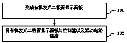
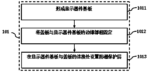
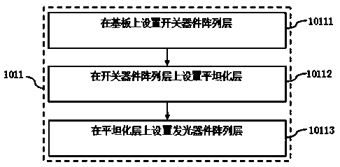
[0022] refer to figure 1 , figure 2 and image 3 , figure 1 It is a flow chart of the manufacturing method of the organic light emitting diode display device of the present invention, figure 2 for figure 1 A flowchart of the steps of forming an organic light emitting diode display panel in , image 3 for figure 2 A flowchart of the steps of forming a display device substrate in .

[0023] The manufacturing method of the organic light emitting diode display device of the present invention comprises the following steps:

[0024] A (step 101 ), forming an organic light emitting diode display panel.

[0025] B (step 102), connecting the organic light emitting diode display panel with the controller and the driving circuit.

[0026] Wherein, the step A includes:

[0027] a1 (step 1011 ), forming a display device substrate.

[0028] a2 (step 1012 ), fixing the cover plate to the edge of the display device substrate, wherein the cover plate covers at least a part of the ...


PUM


Abstract

The invention discloses an organic light emitting diode display device and a manufacturing method of a panel. The method for manufacturing an organic light emitting diode display device includes: A, forming an organic light emitting diode display panel; B, connecting the organic light emitting diode display panel with a controller and a driving circuit; step A includes: a1, forming a display device substrate; a2, placing the cover The panel is fixed to the edge of the display device substrate; a3, a moisture-proof protective layer is provided at the connection between the display device substrate and the cover plate; step a1 includes: a11, a switching device array layer is provided on the substrate; a12, the switching device array layer A planarization layer is arranged on the planarization layer; a13, a light-emitting device array layer is arranged on the planarization layer, and the light-emitting device array layer includes an anode layer, a hole injection layer, a hole transport layer, a light-emitting material layer, an electron transport layer, an electron injection layer, and a cathode layer. The invention can prevent water vapor from being mixed into the display of the organic light-emitting diode.

Description

technical field [0001] The invention relates to the field of display technology, in particular to an organic light emitting diode display device and a method for manufacturing a panel. Background technique [0002] The cover plate and the substrate in the conventional organic light emitting diode display panel form a cavity, and the display device in the above conventional organic light emitting diode display panel is arranged in the cavity. [0003] During the working process of the above-mentioned conventional OLED display panel, water vapor is easily mixed into the chamber. [0004] When a lot of water vapor accumulates in the chamber, the display device will be damaged. [0005] Therefore, in order to make the OLED display panel have a longer service life, it is necessary to keep the chamber dry. Contents of the invention [0006] The object of the present invention is to provide a method for manufacturing an organic light emitting diode display device and a panel, w...

Claims


Application Information

Patent Timeline
Patent Type & Authority Patents(China)
IPC IPC(8): H01L27/32H01L51/56
CPCH10K59/12H10K71/00
Inventor 刘彦龙苏俊武丁杰李涛
Owner 盐城项果科技有限公司
Features
  • R&D
  • Intellectual Property
  • Life Sciences
  • Materials
  • Tech Scout
  • Unparalleled Data Quality
  • Higher Quality Content
  • 60% Fewer Hallucinations
Learn More