Memory element and method of manufacturing the same
A technology for storage elements and manufacturing methods, applied in semiconductor/solid-state device manufacturing, electrical components, semiconductor devices, etc., can solve problems such as difficult process margins, improve sub-channel defects, reduce micro-load effects, and increase margins Effect
- Summary
- Abstract
- Description
- Claims
- Application Information
AI Technical Summary
Problems solved by technology
Method used
Image

Examples
Embodiment Construction
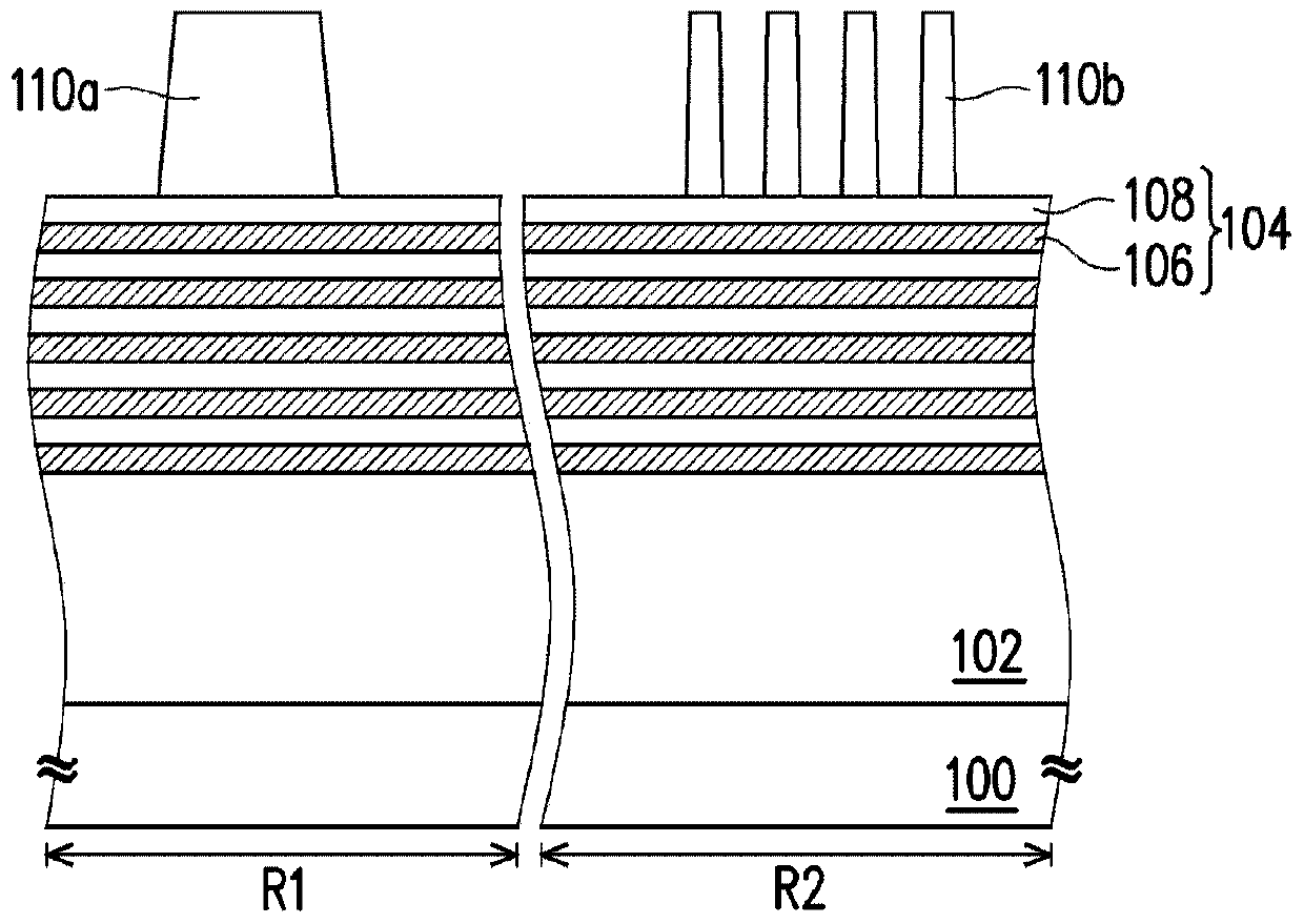
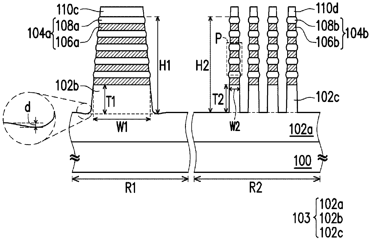
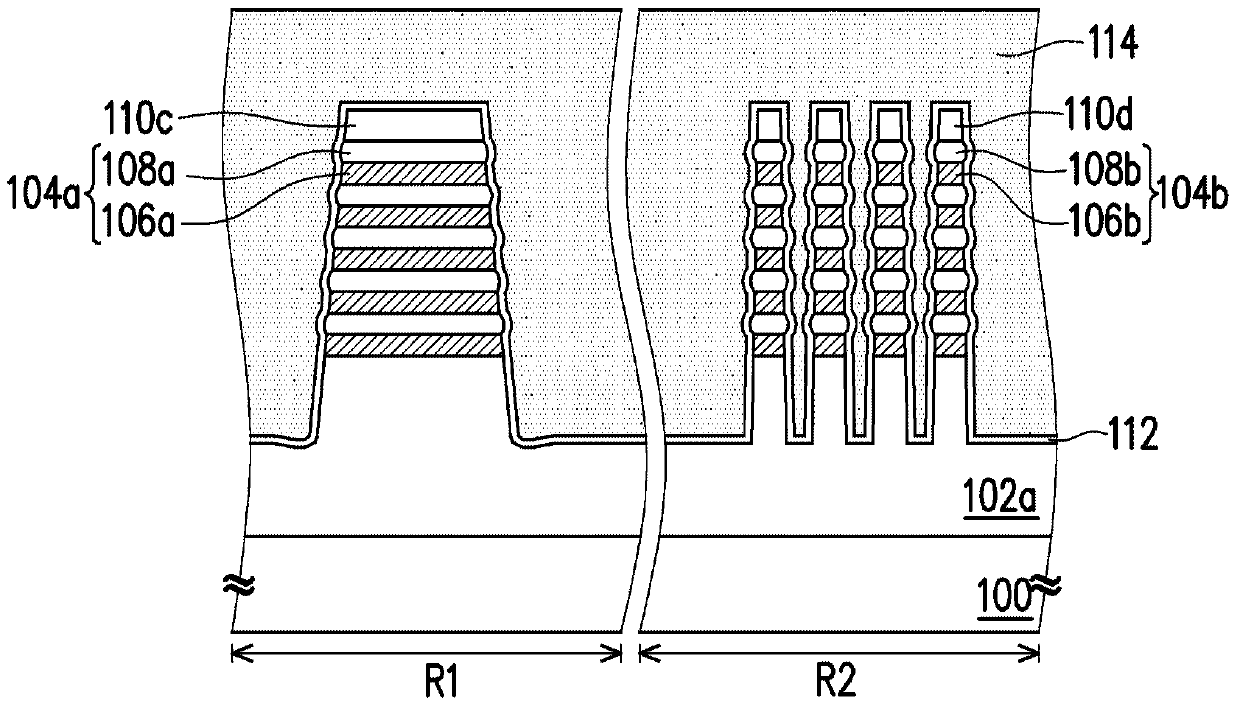
[0041] Figure 1A to Figure 1C It is a schematic cross-sectional view of the manufacturing process of the storage element according to the embodiment of the present invention.
[0042] Please refer to Figure 1A , firstly, a substrate 100 is provided. The substrate 100 has a first region R1 and a second region R2. In this embodiment, the first region R1 may be, for example, a peripheral circuit region, and the second region R2 may be, for example, a memory cell array region. The substrate 100 is, for example, a semiconductor substrate, a semiconductor compound substrate, or a semiconductor substrate on an insulating layer (Semiconductor Over Insulator, S01). Semiconductors are, for example, atoms of group IVA, such as silicon or germanium. The semiconductor compound is, for example, a semiconductor compound formed of atoms of group IVA, such as silicon carbide or germanium silicide, or a semiconductor compound formed of atoms of group IIIA and group VA, such as gallium arse...
PUM
 Abstract
Description
Claims
Application Information
 - R&D
- Intellectual Property
- Life Sciences
- Materials
- Tech Scout
- Unparalleled Data Quality
- Higher Quality Content
- 60% Fewer Hallucinations
Browse by: Latest US Patents, China's latest patents, Technical Efficacy Thesaurus, Application Domain, Technology Topic, Popular Technical Reports.
© 2025 PatSnap. All rights reserved.Legal|Privacy policy|Modern Slavery Act Transparency Statement|Sitemap|About US| Contact US: help@patsnap.com