Check patentability & draft patents in minutes with Patsnap Eureka AI!

Semiconductor structure and formation method thereof

A technology of semiconductor and gate structure, applied in the field of semiconductor structure and its formation, can solve the problems of affecting device performance, dislocation, hot carrier effect on device performance, etc., and achieve the effect of improving recovery ability and reducing impact.

Active Publication Date: 2017-04-19
ZING SEMICON CORP
View PDF5 Cites 0 Cited by
  • Summary
  • Abstract
  • Description
  • Claims
  • Application Information

AI Technical Summary

Problems solved by technology

[0007] However, including but not limited to the semiconductor structure formed through the above steps, dangling bonds will be formed inside. These dangling bonds mainly occur on the surface or interlayer interface, which will cause holes, dislocations, and the introduction of other impurities. situation
[0008] In addition, in the current MOS manufacturing process, another issue that arises is the impact of hot carrier effects on device performance
Special attention is paid to the fact that in smaller-sized devices, when they are used at higher voltages, the carriers in the channel will enter the insulating layer because they have enough energy, thus affecting the performance of the device

Method used


Image

  • Semiconductor structure and formation method thereof
  • Semiconductor structure and formation method thereof
  • Semiconductor structure and formation method thereof

Examples


Embodiment Construction

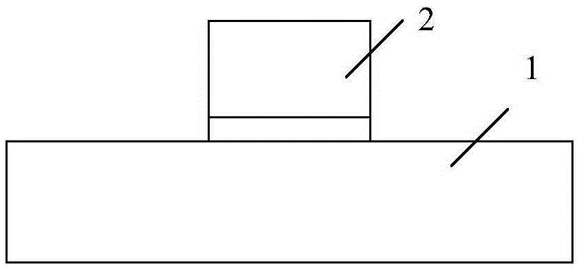
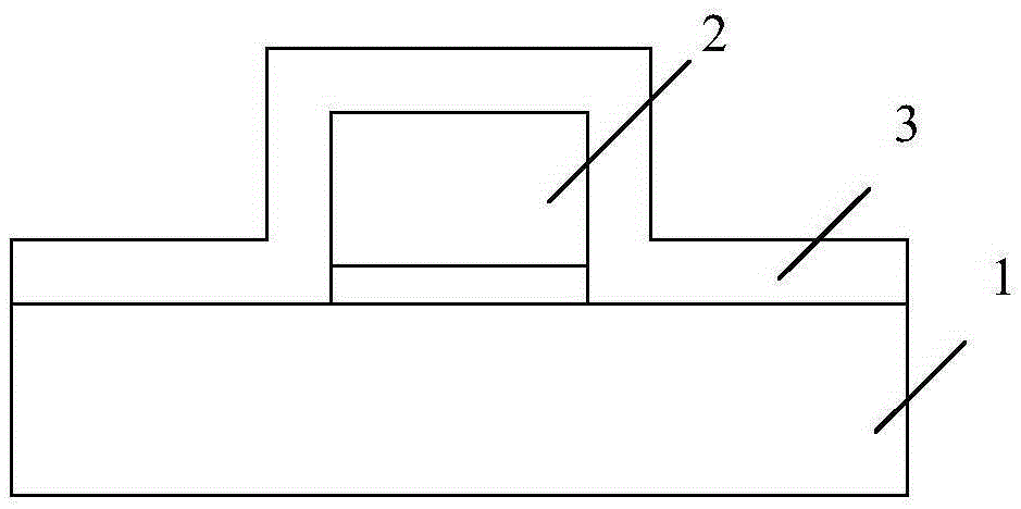
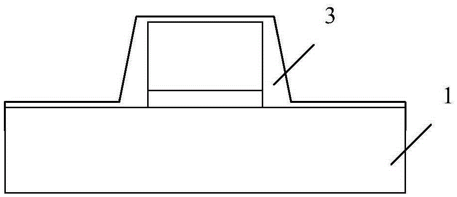
[0028] The semiconductor structure of the present invention and its forming method will be described in more detail below in conjunction with the schematic diagrams, in which the preferred embodiments of the present invention are shown. It should be understood that those skilled in the art can modify the present invention described here and still realize the advantages of the present invention. Favorable effect. Therefore, the following description should be understood to be widely known to those skilled in the art, and not as a limitation to the present invention.

[0029] In the following paragraphs, the present invention is described in more detail by way of example with reference to the drawings. According to the following description and claims, the advantages and features of the present invention will be clearer. It should be noted that the drawings are in a very simplified form and all use imprecise proportions, which are only used to conveniently and clearly assist in ex...


PUM


Abstract

The invention discloses a semiconductor structure and a formation method thereof. The method comprises steps that a substrate having a dummy grid is provided, a deuterium-doped source-drain epitaxial layer is formed at two sides of the dummy grid on the substrate through the gas phase epitaxial deposition process; the dummy grid is removed, a grid structure with a gate oxide is formed at the position of the dummy grid, and deuterium enters the gate oxide. Through the acquired semiconductor structure, as deuterium is made to enter the gate oxide, a stable covalent bond is formed at an interface of the gate oxide, a dangling bond existence problem can be effectively improved, moreover, recovery capability of the device for responding to hot carrier's effects can be improved, and thereby influence of the hot carrier's effects on device performance is reduced.

Description

Technical field [0001] The invention relates to the field of semiconductor manufacturing, in particular to a semiconductor structure and a method of forming the same. Background technique [0002] At present, semiconductor manufacturing technology has been rapidly developed. Such as Figure 1-6 A common MOS formation process in the prior art is shown. include: [0003] Such as figure 1 As shown, a gate structure 2 is formed on the substrate 1; [0004] Such as Figure 2-Figure 4 As described, a protective layer 3 is deposited on the substrate 1 to cover the gate structure 2; reactive ion etching is performed to remove part of the protective layer 3, and the protective layer 3 is inclined at both sides of the gate structure 2; further Remove the part of the protective layer 3 on the substrate 1 to form a gate sidewall 4; [0005] Such as Figure 5 As shown, the source and drain electrodes 5 are epitaxially formed on both sides of the gate 2 on the substrate 1, and doped in-situ; [0...

Claims


Application Information

Patent Timeline
Patent Type & Authority Applications(China)
IPC IPC(8): H01L21/336H01L21/28H01L29/78H01L29/51
CPCH01L21/2822H01L29/51H01L29/66545H01L29/78H01L29/4908H01L29/66772H01L29/78615H01L21/3003
Inventor 肖德元
Owner ZING SEMICON CORP
Features
  • R&D
  • Intellectual Property
  • Life Sciences
  • Materials
  • Tech Scout
  • Unparalleled Data Quality
  • Higher Quality Content
  • 60% Fewer Hallucinations
Learn More