Shift register, its driving method and gate driving circuit
A shift register and gate signal technology, applied in static memory, digital memory information, instruments, etc., can solve the problem of transistor noise removal failure and other problems, to avoid the rise of threshold voltage, improve work stability and reliability , Solve the effect of noise removal failure
- Summary
- Abstract
- Description
- Claims
- Application Information
AI Technical Summary
Problems solved by technology
Method used
Image

Examples
no. 1 example
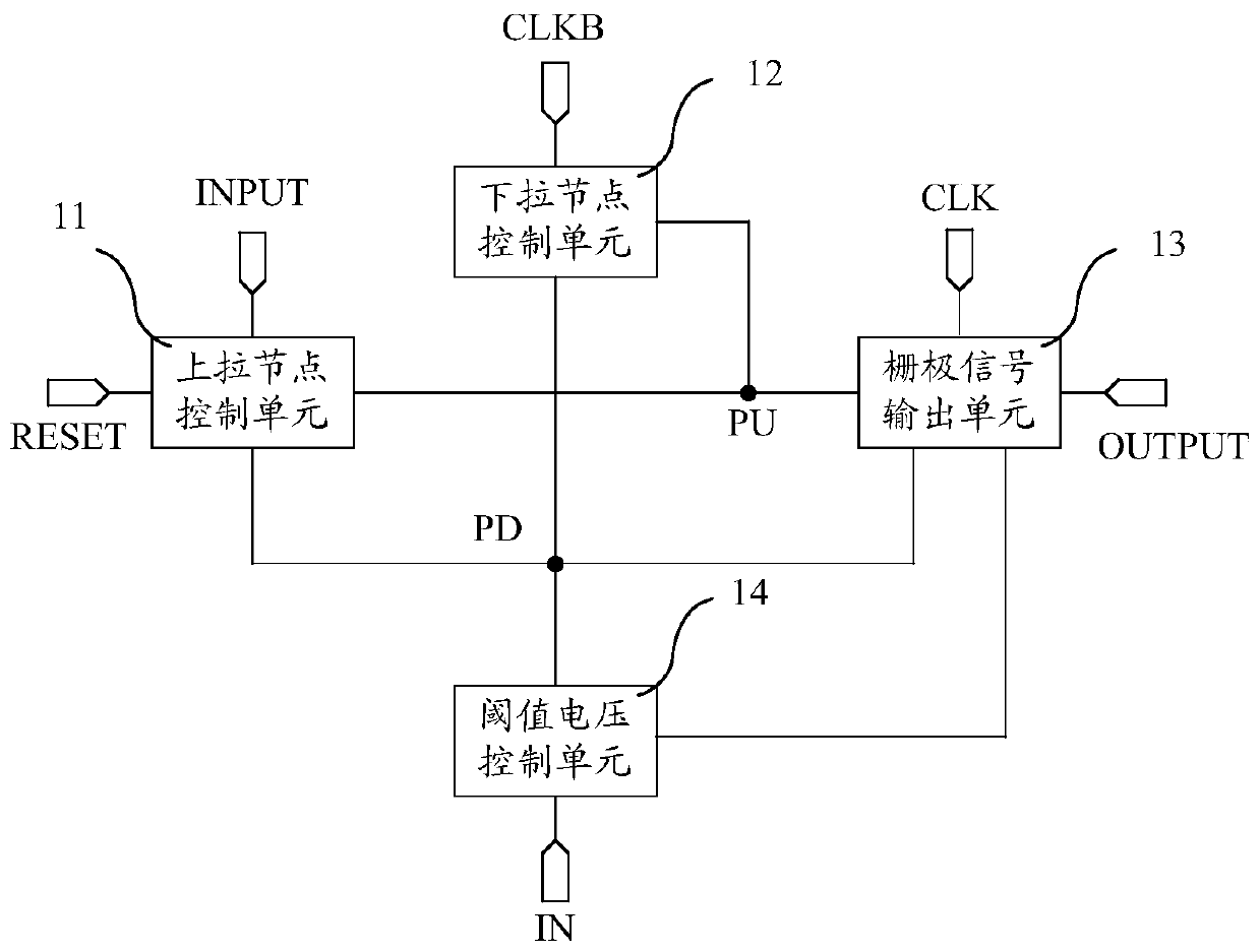
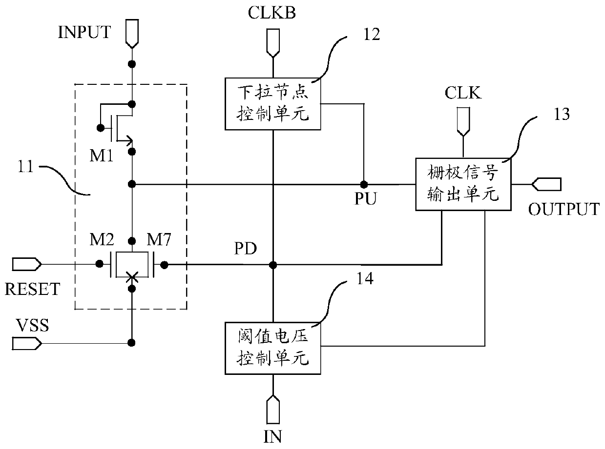
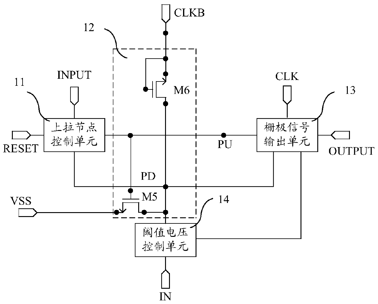
[0065] figure 1 It is a schematic structural diagram of a shift register according to an embodiment of the present invention. Such as figure 1 As shown, the shift register includes: a signal input terminal INPUT, a reset terminal RESET, a first clock input terminal CLK, a second clock input terminal CLKB, a control terminal IN and a signal output terminal OUTPUT, and also includes a pull-up node control unit 11, a pull-down node Node control unit 12, gate signal output unit 13 and threshold voltage control unit 14, wherein:
[0066] The pull-up node control unit 11 is respectively connected to the signal input terminal INPUT, the reset terminal RESET, the pull-up node PU and the pull-down node PD; it is used to control the potential of the pull-up node PU when the input signal of the signal input terminal INPUT is at a high level It is high level; it is also used to control the potential of the pull-up node PU to be low when the input signal of the reset terminal RESET is hi...
no. 2 example
[0109] Based on the inventive concept of the foregoing embodiments, the embodiment of the present invention also provides a driving method of a shift register, Figure 8 It is a flowchart of a driving method of a shift register according to an embodiment of the present invention. Such as Figure 8 As shown, the shift register includes: signal input terminal INPUT, reset terminal RESET, first clock input terminal CLK, second clock input terminal CLKB, control terminal IN, signal output terminal OUTPUT, pull-up node control unit, pull-down node control unit , a gate signal output unit and a threshold voltage control unit, the driving method of the shift register includes:
[0110] Under the control of the signal input terminal, the reset terminal and the second clock input terminal, the node control unit controls the potentials of the pull-up node and the pull-down node;
[0111] Under the control of the first clock input terminal, the pull-up node and the pull-down node, the ...
no. 3 example
[0128] Based on the inventive concepts of the foregoing embodiments, this embodiment further provides a gate driving circuit, which uses the shift register described in the foregoing embodiments.
[0129] Based on the inventive concepts of the foregoing embodiments, this embodiment further provides a display panel, which includes the gate driving circuit described in the foregoing embodiments. The display panel can be any product or component with a display function such as a mobile phone, a tablet computer, a TV set, a monitor, a notebook computer, a digital photo frame, a navigator, and the like.
PUM
 Abstract
Description
Claims
Application Information
 - R&D Engineer
- R&D Manager
- IP Professional
- Industry Leading Data Capabilities
- Powerful AI technology
- Patent DNA Extraction
Browse by: Latest US Patents, China's latest patents, Technical Efficacy Thesaurus, Application Domain, Technology Topic.
© 2024 PatSnap. All rights reserved.Legal|Privacy policy|Modern Slavery Act Transparency Statement|Sitemap