Gallium nitride nanorod LED epitaxial wafer grown on silicon substrate and preparation method for LED epitaxial wafer
A technology of LED epitaxial wafers and gallium nitride nanometers, which is applied in the manufacture of semiconductor/solid-state devices, electrical components, circuits, etc. Effects of defect density, improvement of luminous efficiency, and improvement of radiative recombination efficiency
- Summary
- Abstract
- Description
- Claims
- Application Information
AI Technical Summary
Problems solved by technology
Method used
Image
Examples
Embodiment 1
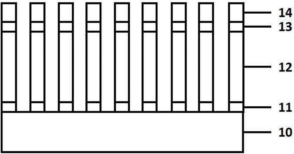
[0035] The preparation method of the gallium nitride nanocolumn LED epitaxial wafer grown on the silicon substrate of this embodiment comprises the following steps:
[0036] (1) Selection of substrate: use ordinary silicon substrate;
[0037] (2) Substrate cleaning: Put the silicon substrate into a mixed solution of hydrofluoric acid and deionized water with a volume ratio of 1:20 and ultrasonically clean it for 2 minutes to remove oxides and dirt particles on the surface of the silicon substrate, and then put it into the deionized water. Ultrasound in deionized water for 2 minutes to remove surface impurities and blow dry with high-purity dry nitrogen;
[0038] (3) Deposition of metal indium droplets: the molecular beam epitaxy growth process was adopted, the substrate temperature was adjusted to 600°C, and the pressure in the reaction chamber was 5.0×10 -5 Pa, under the condition that the growth rate is 0.2ML / s, the metal indium in the indium beam source is annealed while d...
Embodiment 2
[0046] The preparation method of the gallium nitride nanocolumn LED epitaxial wafer grown on the silicon substrate of this embodiment comprises the following steps:
[0047] (1) Substrate: adopt ordinary silicon substrate;
[0048] (2) Substrate cleaning: Put the silicon substrate into a mixed solution of hydrofluoric acid and deionized water with a volume ratio of 1:20 and ultrasonically clean it for 2 minutes to remove oxides and dirt particles on the surface of the silicon substrate, and then put it into the deionized water. Ultrasound in deionized water for 1 minute to remove surface impurities, and blow dry with high-purity dry nitrogen;
[0049] (3) Deposition of metal indium droplets: the molecular beam epitaxy growth process was adopted, the substrate temperature was adjusted to 550°C, and the pressure in the reaction chamber was 5.0×10 -5 Pa, under the condition that the growth rate is 0.2ML / s, the metal indium in the indium beam source is annealed while depositing o...
PUM
| Property | Measurement | Unit |
|---|---|---|
| Height | aaaaa | aaaaa |
| Diameter | aaaaa | aaaaa |
| Height | aaaaa | aaaaa |
Abstract
Description
Claims
Application Information
 - R&D Engineer
- R&D Manager
- IP Professional
- Industry Leading Data Capabilities
- Powerful AI technology
- Patent DNA Extraction
Browse by: Latest US Patents, China's latest patents, Technical Efficacy Thesaurus, Application Domain, Technology Topic, Popular Technical Reports.
© 2024 PatSnap. All rights reserved.Legal|Privacy policy|Modern Slavery Act Transparency Statement|Sitemap|About US| Contact US: help@patsnap.com


