Array substrate and manufacturing method therefor, display panel and display apparatus

A technology of an array substrate and a manufacturing method, applied in the display field, can solve the problems of electrostatic removal, small width, large resistance, etc., and achieve the effect of preventing ESD and reducing resistance

Inactive Publication Date: 2017-08-01
BOE TECH GRP CO LTD +1
View PDF4 Cites 4 Cited by
  • Summary
  • Abstract
  • Description
  • Claims
  • Application Information

AI Technical Summary

Problems solved by technology

However, the design of the narrow frame will cause the width of the peripheral area of ​​the substrate to be small, which will result in a small width of the grounding line

Method used


Image

  • Array substrate and manufacturing method therefor, display panel and display apparatus
  • Array substrate and manufacturing method therefor, display panel and display apparatus
  • Array substrate and manufacturing method therefor, display panel and display apparatus

Examples


Example Embodiment

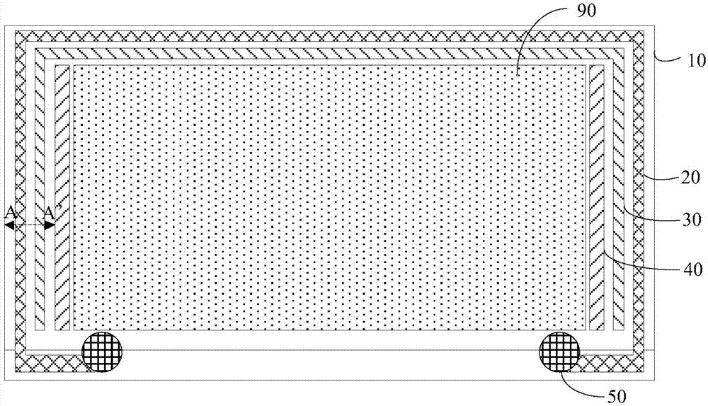
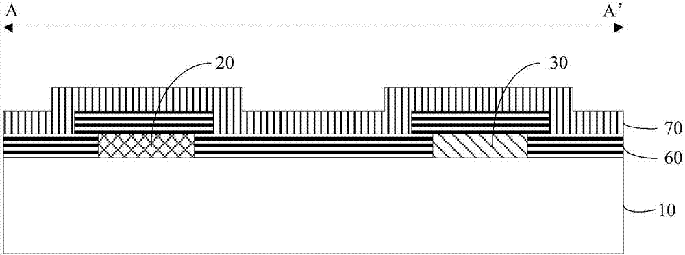
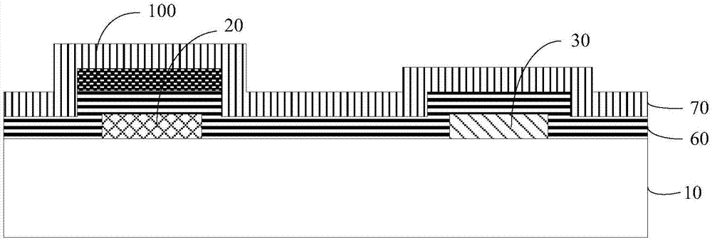
[0038] Example embodiments will now be described more fully with reference to the accompanying drawings. However, the example embodiments can be implemented in various forms, and should not be construed as being limited to the examples set forth herein; on the contrary, the provision of these embodiments makes the present disclosure more comprehensive and complete, and fully conveys the concept of the example embodiments To those skilled in the art. The described features, structures or characteristics can be combined in one or more embodiments in any suitable way. In the following description, many specific details are provided to give a sufficient understanding of the embodiments of the present disclosure. However, those skilled in the art will realize that the technical solutions of the present disclosure can be practiced without one or more of the specific details, or other methods, components, devices, steps, etc. can be used. In other cases, the known technical solution...


PUM


Abstract

The invention discloses an array substrate and a manufacturing method therefor, a display panel and a display apparatus. The array substrate comprises a gate metal layer, a gate insulating layer and a conducive layer structure, wherein the gate metal layer is arranged on the substrate and the gate metal layer comprises a grounding wire positioned in the peripheral region; the gate insulating layer at least covers the gate metal layer; and the conducive layer structure is positioned above the gate insulating layer and the conducive layer structure comprises auxiliary grounding wires positioned in the peripheral region, wherein the auxiliary grounding wires and the grounding wire are connected. By virtue of the embodiments disclosed in the invention, ESD can be prevented more effectively.

Description

technical field [0001] The present disclosure relates to the field of display technology, and in particular, to an array substrate, a method for manufacturing the array substrate, a display panel, and a display device. Background technique [0002] With the development of the information society, people have higher and higher requirements for display devices, which prompts the research on display technology to continue to deepen. At the same time, more and more attention has been paid to the appearance of the display device. Among them, as a design trend, narrow bezels have almost spread throughout the entire display field. For a panel of the same size, the narrow bezel product has a larger screen display area, allowing users to obtain better visual effects, and the appearance of the product is more beautiful and fashionable. In addition, when the display device requires double-screen splicing, the narrow bezel can achieve better splicing effect. [0003] During the test ...

Claims


Application Information

Patent Timeline
IPC IPC(8): H01L23/60H01L27/12H01L21/84
CPCH01L23/60H01L27/124H01L27/1259H01L27/0288H01L27/0296H01L27/0248
Inventor 谷晓芳马小叶王锡平
Owner BOE TECH GRP CO LTD
Why Eureka
Try Eureka