OLED display substrate, manufacturing method therefor, and display device
A display substrate and manufacturing method technology, which is applied in semiconductor/solid-state device manufacturing, semiconductor devices, electrical components, etc., can solve problems affecting the light extraction efficiency of OLED devices, and achieve the effect of improving light extraction efficiency
- Summary
- Abstract
- Description
- Claims
- Application Information
AI Technical Summary
Problems solved by technology
Method used
Image

Examples
Embodiment 1
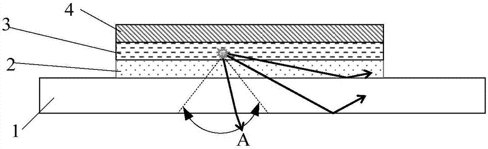
[0072] like Figure 4 As shown, a groove structure is formed on the pixel defining layer 6 surrounding the sub-pixel area of the display substrate, and the depth of the groove structure is equal to the thickness of the pixel defining layer 6 . A reflective layer 7 is formed on the side wall of the groove structure, and the slope angle θ of the side wall of the groove structure is defined by pixels. After the waveguide mode light in the layer is deflected and turned, as much as possible enters the exit cone A2 and becomes the exit mode light selection of principles.
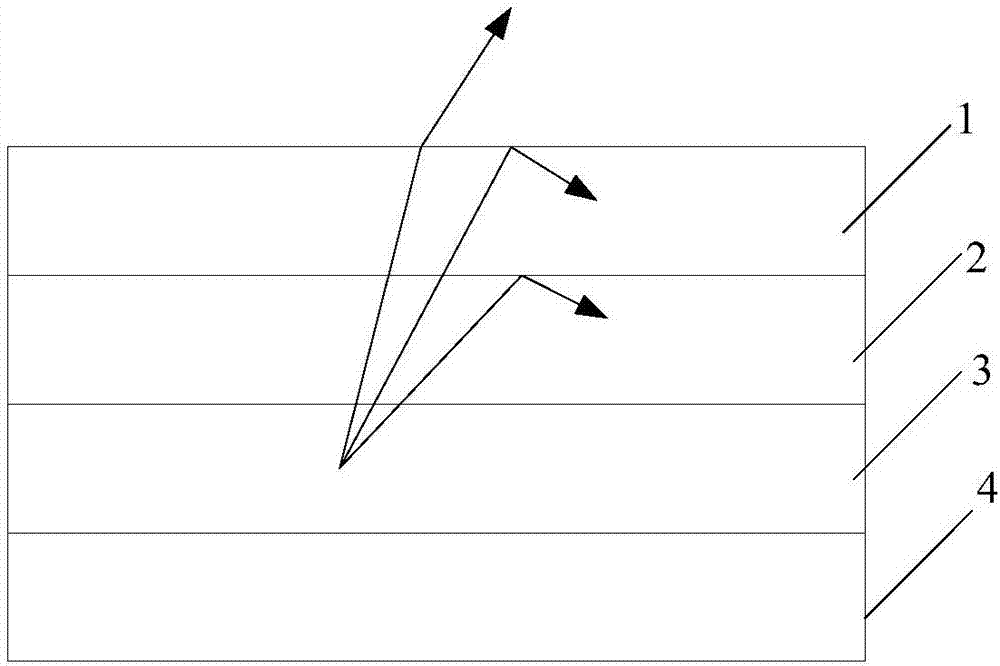
[0073] If no light-emitting structure is prepared, only the light emitted by the organic light-emitting layer 3 within the exit cone A1 can become the outgoing mode light. The terminals of the light-emitting layer 3 and the transparent electrode 2 enter the pixel defining layer 6, and then transmit to the light-reflecting layer 7 in the pixel defining layer 6 and are turned by reflection. After turning, part of...
Embodiment 2
[0076] like Figure 5 As shown, a pixel defining layer 6 on the base substrate 1 is formed between adjacent sub-pixel regions, a thin film transistor array layer 5 is not provided in the peripheral region of the sub-pixel, and a groove is formed on the pixel defining layer 6 surrounding the sub-pixel region structure, the depth of the groove structure is equal to the sum of the thicknesses of the pixel defining layer 6 and the thin film transistor array layer 5 . A reflective layer 7 is formed on the side wall of the groove structure, and the slope angle θ of the side wall of the groove structure is defined by pixels. After the waveguide mode light in the layer is reflected and turned, as much as possible enters the exit cone A2, becoming Principle selection.
[0077] The display substrate of this embodiment has no thin film transistor array layer mode light, and the waveguide mode light only has organic light emitting layer / transparent electrode mode light and substrate subs...
Embodiment 3
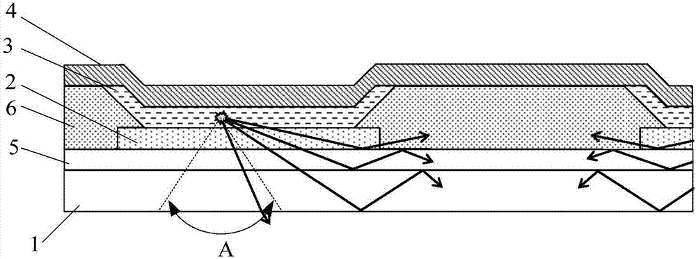
[0080] like Figure 8 As shown, a pixel defining layer 6 on the base substrate 1 is formed around the sub-pixel area, and a thin film transistor array layer 5 is also provided in the sub-pixel surrounding area, and the pixel defining layer 6 surrounding the sub-pixel area and the thin film transistor array layer 5 are composed of A groove structure is formed on the stack structure, and the depth of the groove structure is equal to the sum of the thicknesses of the pixel defining layer 6 and the thin film transistor array layer 5 . A reflective layer 7 is formed on the side wall of the groove structure, and the groove structure corresponds to the slope angle θ of the side wall of the pixel defining layer 6 1 , The groove structure corresponds to the slope angle θ of the side wall of the thin film transistor array layer 5 2 After the waveguide-mode light in the pixel-defining layer and the thin-film transistor array layer is deflected by reflection, as many parts as possible en...
PUM
 Abstract
Description
Claims
Application Information
 - R&D Engineer
- R&D Manager
- IP Professional
- Industry Leading Data Capabilities
- Powerful AI technology
- Patent DNA Extraction
Browse by: Latest US Patents, China's latest patents, Technical Efficacy Thesaurus, Application Domain, Technology Topic.
© 2024 PatSnap. All rights reserved.Legal|Privacy policy|Modern Slavery Act Transparency Statement|Sitemap