Check patentability & draft patents in minutes with Patsnap Eureka AI!

III-nitride nanowire led with strain modified surface active region and method of making thereof

A technology of active regions and nanowires, applied in electrical components, circuits, semiconductor devices, etc., can solve the problems of low efficiency of light-emitting diodes and reduced efficiency of photon recombination

Inactive Publication Date: 2017-10-13
GLO
View PDF4 Cites 5 Cited by
  • Summary
  • Abstract
  • Description
  • Claims
  • Application Information

AI Technical Summary

Problems solved by technology

[0005] U.S. Patent No. 8,138,493, issued March 20, 2012, which is hereby incorporated by reference in its entirety, states that it is difficult to build LEDs in the infrared to green wavelength region using conventional planar technology in GaN systems, and that these LEDs Efficacy is much lower than that of blue-emitting LEDs
This can be attributed to: a) the miscibility gap of the InGaN material in the red and green wavelength regions, since it is theoretically expected to have an In of about 0.4x Ga 1-x N is not a stable material; and b) the high intrinsic defect density of the planar layers of the LED structure reduces photon recombination efficacy to a significantly higher extent for high In content InGaN than for low In content InGaN used in blue LEDs

Method used


Image

  • III-nitride nanowire led with strain modified surface active region and method of making thereof
  • III-nitride nanowire led with strain modified surface active region and method of making thereof
  • III-nitride nanowire led with strain modified surface active region and method of making thereof

Examples


Embodiment Construction

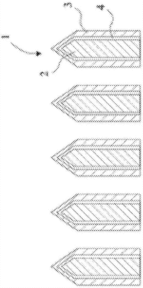
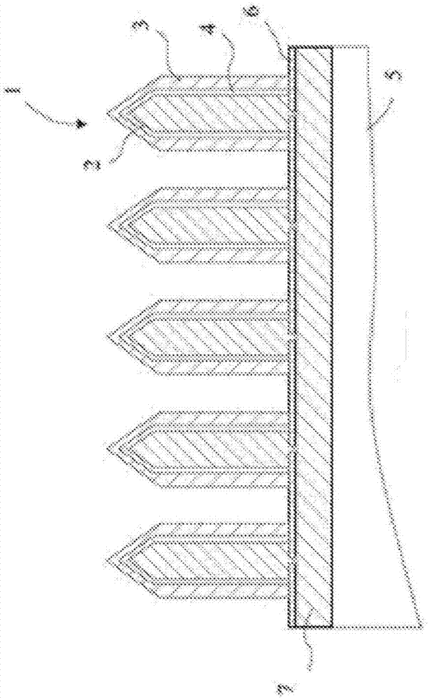
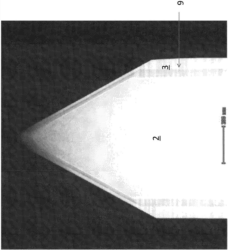
[0013] In one embodiment, the active area shell is formed on a non-uniform surface such that the active area shell has a non-uniform profile (e.g., non-vertical radial sidewalls and / or a gradient in the horizontal direction with respect to the vertical direction). uneven thickness that varies with height). This "corrugated" surface reduces or eliminates defects (such as stack-up defects) in the outer shell.

[0014] Formation of an active region shell comprising one or more In(Al)GaN / (Al)GaN quantum wells on a non-uniform surface results in the formation of an indium-rich In(Al)GaN region by self-assembly during formation of the active region (eg InGaN or InAlGaN regions with more than 10 atomic percent indium, such as 15 to 35 atomic percent indium). Depending on the indium content of the regions, it is believed that these indium-rich regions are responsible for longer wavelength spectral regions (e.g., green to yellow 495-590 nm peak emission wavelength region and / or orange...


PUM

PropertyMeasurementUnit
thicknessaaaaaaaaaa
thicknessaaaaaaaaaa
thicknessaaaaaaaaaa

Abstract

A core- shell nanowire device includes an eave region having a structural discontinuity from the p-plane in the upper tip portion of the shell to the m-plane in the lower portion of the shell. The eave region has at least 5 atomic percent higher indium content than the p-plane and m-plane portions of the shell.

Description

[0001] Related applications [0002] This application claims priority to US Provisional Application No. 62 / 036,363, filed August 12, 2014, which is hereby incorporated by reference in its entirety. technical field [0003] Embodiments of the present invention relate generally to semiconductor devices, such as nanowire light emitting diodes (LEDs), and in particular, to nanowire LEDs having non-uniform active regions. Background technique [0004] As an alternative to planar LEDs, nanowire light-emitting diodes (LEDs) have received increasing attention. Compared to LEDs fabricated by conventional planar technologies, nanowire LEDs offer unique properties due to the one-dimensional nature of the nanowires, improved flexibility in material combinations due to less lattice-matching constraints, and at larger Opportunities for processing on substrates. [0005] U.S. Patent No. 8,138,493, issued March 20, 2012, which is hereby incorporated by reference in its entirety, states t...

Claims


Application Information

Patent Timeline
Patent Type & Authority Applications(China)
IPC IPC(8): H01L33/02H01L33/26
CPCH01L33/24H01L33/007H01L33/025H01L33/06H01L33/08H01L33/12H01L33/18H01L33/32H01L33/42
Inventor 琳达·罗马诺王平
Owner GLO
Features
  • R&D
  • Intellectual Property
  • Life Sciences
  • Materials
  • Tech Scout
  • Unparalleled Data Quality
  • Higher Quality Content
  • 60% Fewer Hallucinations
Learn More