Input undervoltage protection circuit
A protection circuit, input undervoltage technology, applied in emergency protection circuit devices, protection against undervoltage or no voltage, DC power input conversion to DC power output, etc., can solve the waste of PCB board area and increase the number of resistors Increased number and package size, etc., to reduce design difficulty, reduce resistance, and reduce power loss
- Summary
- Abstract
- Description
- Claims
- Application Information
AI Technical Summary
Problems solved by technology
Method used
Image

Examples
Embodiment 1
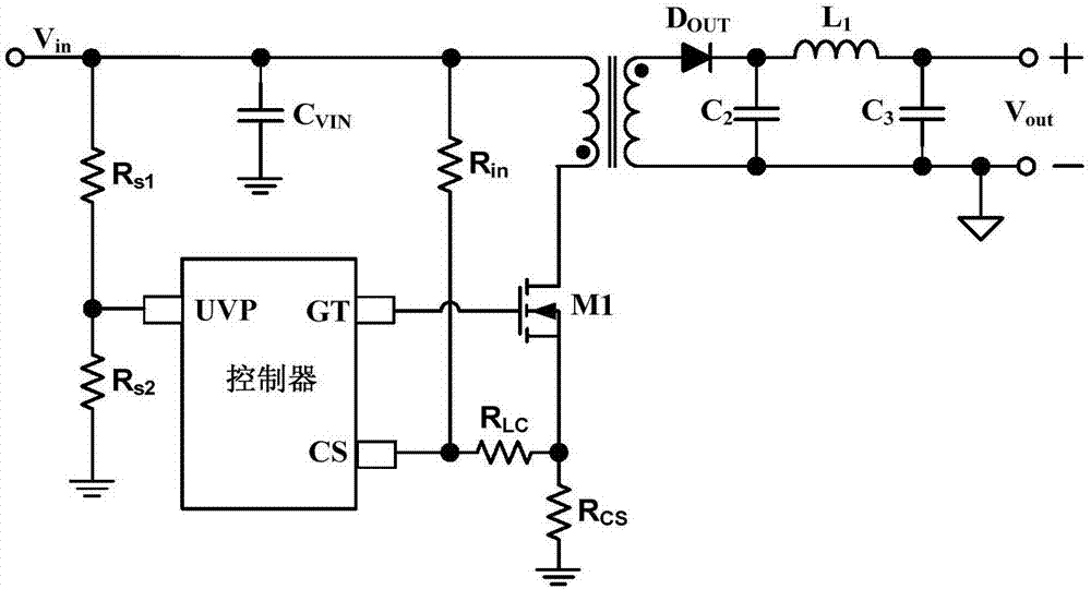
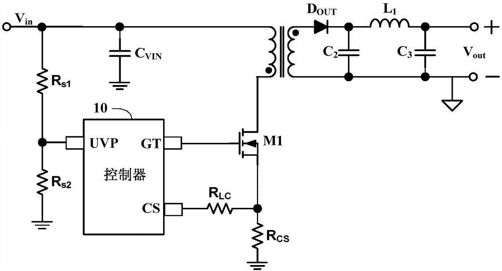
[0029] figure 2 It is a simplified diagram of the application circuit of the present invention. The input undervoltage protection circuit described in the present invention is a circuit in the controller 10, and other circuits in the controller 10 are irrelevant to the present invention and will not be described here. figure 2 The main power topology is a well-known technology, including the input voltage V in , output voltage V out , capacitance C VIN , Voltage divider resistor R s1 and R s2 , controller 10, main power transformer, main power tube M1, diode D OUT , capacitance C 2 , inductance L 1 and capacitance C 3 and other components. The GT pin is the drive output of the controller 10, which is used to control the turn-on and turn-off of the power transistor M1; the CS pin detects the current sampling resistor R CS The voltage to determine the peak current flowing through the power tube M1; the UVP pin is the detection pin of the input undervoltage protection,...
Embodiment 2
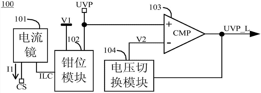
[0054] The difference from Embodiment 1 is that the clamping module 202 of Embodiment 2 further includes a PMOS transistor PM3 and an NMOS transistor NM4 . The source of PM3 is connected to the pin UVP, the gate is connected to the gate of PM1, the drain is connected to the gate and drain of NM4; the source of NM4 is connected to the reference ground.
[0055] Because of the addition of this current branch where PM3 is located, the current I that can be released by the clamp module 202 UVP larger, compared with the clamping module 102 of Embodiment 1, the voltage divider resistor R s1 Under the same conditions, the clamping module 202 is applicable to a wider input voltage range. In order to facilitate the description of the circuit principle, the width-to-length ratios of the NMOS transistors NM2 and NM3 of the clamping module 202 are the same, and the ratio of the width-to-length ratios of the PMOS transistors PM2 and PM3 is
[0056]
[0057] So the current I of Example...
PUM
 Abstract
Description
Claims
Application Information
 - Generate Ideas
- Intellectual Property
- Life Sciences
- Materials
- Tech Scout
- Unparalleled Data Quality
- Higher Quality Content
- 60% Fewer Hallucinations
Browse by: Latest US Patents, China's latest patents, Technical Efficacy Thesaurus, Application Domain, Technology Topic, Popular Technical Reports.
© 2025 PatSnap. All rights reserved.Legal|Privacy policy|Modern Slavery Act Transparency Statement|Sitemap|About US| Contact US: help@patsnap.com