Wafer annealing device
An annealing device and wafer technology, applied in electrical components, semiconductor/solid-state device manufacturing, circuits, etc., can solve the problems of reducing the service life of heating bulbs, heating bulbs damage, etc., to improve production rhythm, reduce the probability of damage, improve The effect of the service life
- Summary
- Abstract
- Description
- Claims
- Application Information
AI Technical Summary
Problems solved by technology
Method used
Image

Examples
Example
[0031] First embodiment
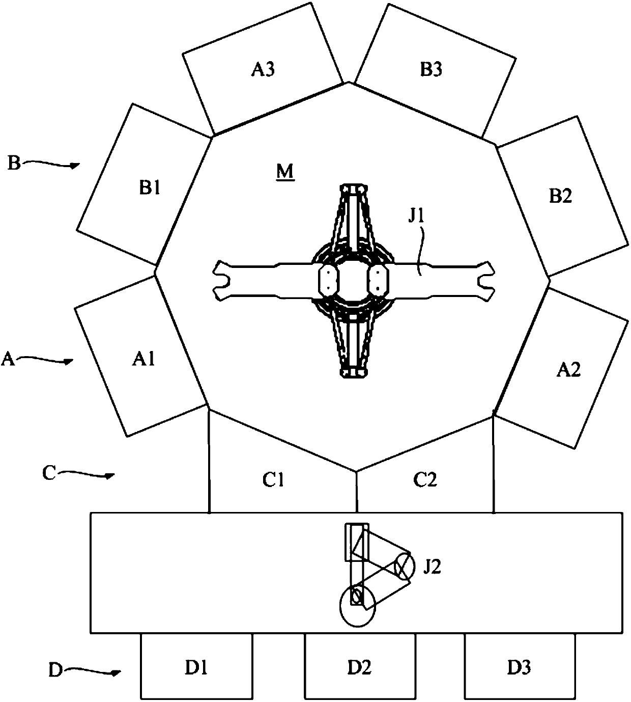
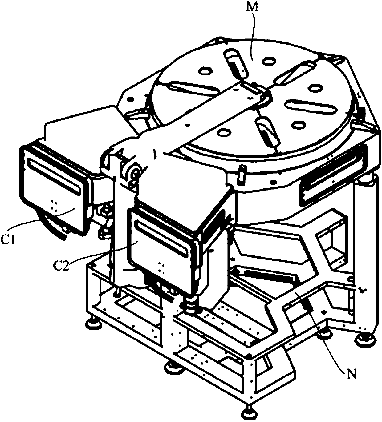
[0032] Reference figure 1 , figure 2 , A wafer annealing device, including a transfer platform M, a preheating chamber A, a process chamber B and a cooling chamber C ( figure 2 The preheating chamber A and the process chamber B are not shown in the figure. The preheating chamber A, the process chamber B and the cooling chamber C are fixedly arranged on the transfer platform M along the circumferential direction of the transfer platform M. Among them, the wafer annealing device includes three preheating chambers A, three process chambers B, and two cooling chambers C, which are preheating chamber A1, preheating chamber A2, preheating chamber A3, and process Chamber B1, process chamber B2, process chamber B3 and cooling chamber C1, cooling chamber C2.
[0033] The wafer annealing device also includes three wafer storage chambers D and two transfer mechanisms, namely wafer storage chamber D1, wafer storage chamber D2, wafer storage chamber D3, first transfe...
Example
[0062] Second embodiment
[0063] Reference Figure 5 The difference between this embodiment and the first embodiment is that the wafer annealing device includes four preheating chambers A and two process chambers B, which are preheating chamber A1, preheating chamber A2, and preheating chamber A2. Thermal chamber A3, preheat chamber A4, process chamber B1, and process chamber B2.
[0064] Among them, the preheating chamber A1 and the preheating chamber A3 correspond to the process chamber B1, and the process of transferring the wafer by the first transfer mechanism J1 is: cooling chamber C, preheating chamber A1 or preheating chamber A3, Process chamber B1, and finally return to cooling chamber C.
[0065] The preheating chamber A2 and the preheating chamber A4 correspond to the process chamber B2. The process of transferring the wafer by the first transfer mechanism J1 is as follows: cooling chamber C, preheating chamber A2 or preheating chamber A4, process chamber B2, and finall...
Example
[0081] The third embodiment
[0082] Reference Image 6 The difference between this embodiment and the first embodiment is that the wafer annealing device includes two preheating chambers A and four process chambers B, which are preheating chamber A1, preheating chamber A2, and Chamber B1, process chamber B2, process chamber B3, and process chamber B4.
[0083] Among them, the preheating chamber A1 corresponds to the process chamber B1 and the process chamber B3. The process of transferring the wafer by the first transfer mechanism J1 is: cooling chamber C, preheating chamber A1, process chamber B1 or process chamber Room B3, and finally return to cooling chamber C.
[0084] The preheating chamber A2 corresponds to the process chamber B2 and the process chamber B4. The process of transferring the wafer by the first transfer mechanism J1 is as follows: cooling chamber C, preheating chamber A2, process chamber B2 or process chamber B4, and finally back to cooling chamber C.
[0085] R...
PUM
 Abstract
Description
Claims
Application Information
 - R&D Engineer
- R&D Manager
- IP Professional
- Industry Leading Data Capabilities
- Powerful AI technology
- Patent DNA Extraction
Browse by: Latest US Patents, China's latest patents, Technical Efficacy Thesaurus, Application Domain, Technology Topic.
© 2024 PatSnap. All rights reserved.Legal|Privacy policy|Modern Slavery Act Transparency Statement|Sitemap