Supercharge Your Innovation With Domain-Expert AI Agents!

Seed crystal treatment method and silicon carbide crystal growth method

A technology of crystal growth and processing methods, applied in crystal growth, single crystal growth, single crystal growth, etc.

Inactive Publication Date: 2018-05-11
BEIJING SEVENSTAR ELECTRONICS CO LTD
View PDF6 Cites 11 Cited by
  • Summary
  • Abstract
  • Description
  • Claims
  • Application Information

AI Technical Summary

Problems solved by technology

[0006] The present invention aims to solve at least one of the technical problems existing in the prior art, and proposes a seed crystal treatment method and a silicon carbide crystal growth method for silicon carbide crystal growth, to remove pollution on the seed crystal growth surface, process damage and the own defects of the seed crystal, therefore, silicon carbide crystals with better performance can be grown on the treated seed crystal

Method used


Image

  • Seed crystal treatment method and silicon carbide crystal growth method
  • Seed crystal treatment method and silicon carbide crystal growth method
  • Seed crystal treatment method and silicon carbide crystal growth method

Examples


Embodiment 1

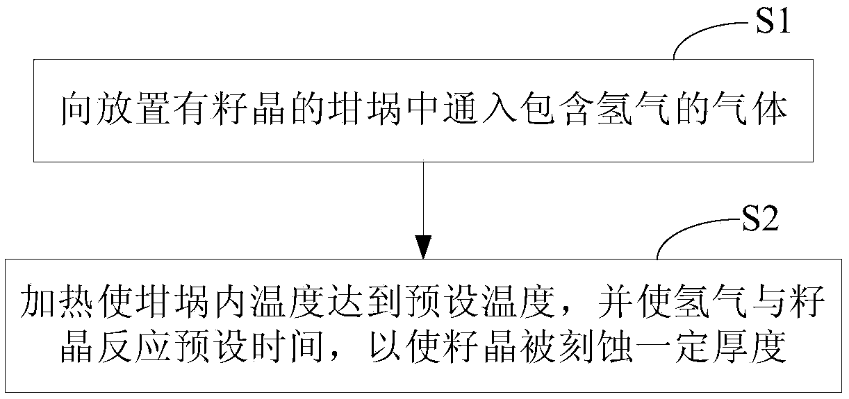
[0036] figure 1 For the working flow diagram of the seed crystal treatment method for silicon carbide crystal growth provided by the embodiment of the present invention, please refer to figure 1 , the seed crystal treatment method for silicon carbide crystal growth provided by the embodiment of the present invention includes the following steps:

[0037] S1, passing a gas containing hydrogen into the crucible on which the seed crystal is placed.

[0038] Specifically, in practical applications, the crucible is generally placed in a crystal growth furnace, and the crucible is generally made of graphite material, and the graphite material has gas permeability, which makes the crystal growth furnace and the crucible actually in a gas communication state. Therefore, In step S1, the gas may be directly fed into the crystal growth furnace, and the gas may pass through the graphite material and enter the crucible.

[0039] S2, heating to make the temperature inside the crucible rea...
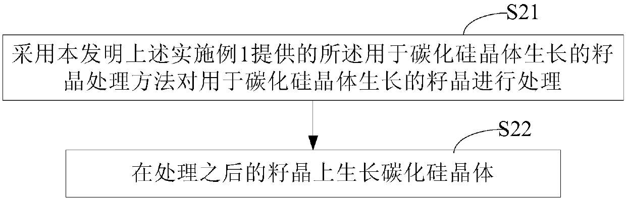
example 1

[0053] Example 1, a silicon carbide seed crystal was fixed on the top of a crucible, and the crucible was placed in a crystal growth furnace. Control the pressure in the crystal growth furnace to be maintained at 10000 Pa, and the temperature rises to 1500 ° C, directly feed a mixed gas of 20% (hydrogen content) hydrogen and argon into the crystal furnace, etch the seed crystal for 2 hours (hours), and finally, The growth surface of the seed crystal can remove surface pollution, scratches and some defects.

example 2

[0054]Example 2, the silicon carbide seed crystal was fixed on the top of the crucible, and the crucible was placed in the crystal growth furnace. Control the pressure in the crystal growth furnace to keep at 1000 Pa, raise the temperature to 1600°C, directly feed the gas containing only hydrogen into the crucible, etch the seed crystal for 1 hour (hour), and finally, the growth surface of the seed crystal can remove surface pollution, Scratches and partial defects.


PUM


Abstract

The invention provides a seed crystal treatment method for silicon carbide crystal growth, and a silicon carbide crystal growth method. The seed crystal treatment method comprises: introducing hydrogen-containing gas into a crucible filled with seed crystal; and heating the crucible to achieve a predetermined temperature, and carrying out a reaction on the hydrogen and the seed crystal for a predetermined time so as to etch the seed crystal a certain thickness. With the seed crystal treatment method and the silicon carbide crystal growth method of the present invention, the pollution on the seed crystal growth surface, the processing damage and the defect of the seed crystal can be removed, such that the silicon carbide crystal with good performance can grow on the treated seed crystal.

Description

technical field [0001] The invention belongs to the technical field of silicon carbide growth, and in particular relates to a seed crystal treatment method for growing silicon carbide crystals and a method for growing silicon carbide crystals. Background technique [0002] As a third-generation semiconductor material, silicon carbide has excellent physical and chemical properties, and has broad application prospects and market space in the fields of high-end optoelectronics, high power, and microwave radio frequency. [0003] At present, the physical vapor transport method (abbreviated as PVT) is the most mature and common method. The working principle of the PVT method is mainly as follows: place the silicon carbide raw material on the bottom of the crucible, fix the seed crystal on the top wall of the crucible, and sublimate the raw material at high temperature (for example, above 2200°C) and low pressure. The sublimation gas uses the thermal field of the crystal The temp...

Claims


Application Information

Patent Timeline
Patent Type & Authority Applications(China)
IPC IPC(8): C30B23/00C30B29/36
CPCC30B23/00C30B29/36
Inventor 李龙远
Owner BEIJING SEVENSTAR ELECTRONICS CO LTD
Features
  • R&D
  • Intellectual Property
  • Life Sciences
  • Materials
  • Tech Scout
  • Unparalleled Data Quality
  • Higher Quality Content
  • 60% Fewer Hallucinations
Learn More