Defect detection method and detection device of printed circuit board and storage medium

A technology for printed circuit boards and detection methods, applied in image data processing, instruments, biological neural network models, etc., can solve the problems of high false alarm rate and low detection efficiency of circuit board defects, and achieve the effect of improving efficiency and accuracy.

Inactive Publication Date: 2018-05-29
川亿电脑(深圳)有限公司
View PDF2 Cites 13 Cited by
  • Summary
  • Abstract
  • Description
  • Claims
  • Application Information

AI Technical Summary

Problems solved by technology

[0005] The main purpose of the present invention is to provide a detection method, detection device and storage medium for printed

Method used


Image

  • Defect detection method and detection device of printed circuit board and storage medium
  • Defect detection method and detection device of printed circuit board and storage medium
  • Defect detection method and detection device of printed circuit board and storage medium

Examples


Example Embodiment

[0040] It should be understood that the specific embodiments described herein are only used to explain the present invention, but not to limit the present invention.

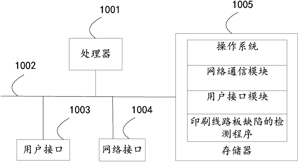
[0041] Reference figure 1 , figure 1 It is a schematic diagram of the structure of the detection device of the hardware operating environment involved in the solution of the embodiment of the present invention.

[0042] Such as figure 1 As shown, the detection device may include: a processor 1001, the processor may be a central processing unit (Central Processing Unit, CPU), a graphics processing unit (Graphics Processing Unit, GPU), or a tensor processing unit Tensor Procession Unit (TPU) and Field Programmable Gate Array (FPGA), communication bus 1002, user interface 1003, network interface 1004, memory 1005. Among them, the communication bus 1002 is used to implement connection and communication between these components. The user interface 1003 may include a display screen (Display) and an input unit such as a ke...


PUM


Abstract

The invention discloses a defect detection method and detection device of a printed circuit board and a storage medium. The detection device carries out image scanning on a to-be-detected printed circuit board to obtain a current image of the to-be-detected printed circuit board; the current image is compared with a preset standard image to obtain a to-be-identified region in the current image; and defect recognition is carried out on the to-be-identified region by a preset neural network model to obtain an identification result of the to-be-identified region. Because defect recognition is carried out on the to-be-identified region by the trained neural network model, the circuit board defect recognition efficiency and accuracy are improved.

Description

technical field [0001] The invention relates to the field of circuit boards, in particular to a detection method, a detection device and a storage medium for defects of a printed circuit board. Background technique [0002] At present, the method used by printed circuit board manufacturers to detect circuit defects is mainly to use the image converted from the design drawing as a template for comparison information, and perform automatic optical scanning on each subsequent printed circuit board to determine the difference point exceeding the set error threshold. For defects, this method will generate a large proportion of false positives, and the defects that really need to be repaired only account for 2% to 10%. It takes a lot of manpower and material resources to filter the false positives, and the efficiency is too low, resulting in waste of resources. . [0003] In addition, the traditional detection method is too rigid, the detection results will not be fed back, and t...

Claims


Application Information

Patent Timeline
IPC IPC(8): G06T7/00G06N3/02
CPCG06N3/02G06T7/001G06T2207/20084G06T2207/30141
Inventor 樊智勇黄龙光
Owner 川亿电脑(深圳)有限公司
Why Eureka
Try Eureka