Resistive random access memory storage unit, manufacturing method thereof, and electronic device
A random access memory and storage unit technology, applied in resistive random access memory storage unit and fabrication method thereof, and the fields of electronic devices, can solve problems such as difficulty in increasing the storage density of conductive bridge random access memory, and achieve improved storage density, good performance, and low cost. Effect
- Summary
- Abstract
- Description
- Claims
- Application Information
AI Technical Summary
Problems solved by technology
Method used
Image

Examples
Embodiment 1
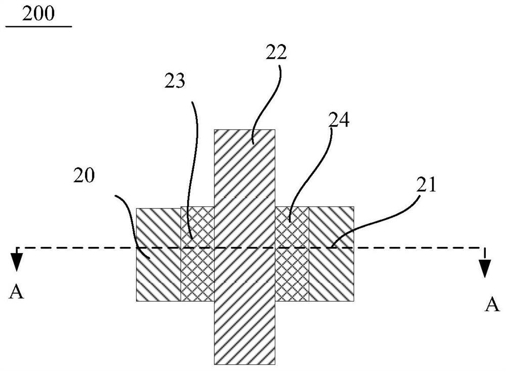
[0039] This embodiment proposes a resistive random access memory storage unit, such as Figure 2A with Figure 2B As shown, the resistive random access memory unit 200 includes a first left electrode 20, a first right electrode 21, a second electrode 22, a first resistive layer 23 and a second resistive layer 24, and the second electrode 22 is arranged in the middle , the first left electrode 20 and the first right electrode 21 are respectively located on both sides of the second electrode 22, the first resistive layer 23 is formed between the first left electrode 20 and the second electrode 22, and the second resistive layer 24 is arranged on Between the first right electrode 21 and the second electrode 22, when different levels are applied to the first left electrode 20, the first right electrode 221, and the second electrode 22, the first resistive variable layer 23 and the second resistive variable layer The resistance of 24 will change. That is, in this embodiment, the ...
Embodiment 2
[0046] The following will refer to image 3 , Figure 4A ~ Figure 4O as well as Figure 5 The manufacturing method of the RRAM storage unit according to an embodiment of the present invention is described in detail. in, image 3 It shows a schematic flow chart of steps of a manufacturing method of a resistive random access memory unit according to an embodiment of the present invention; Figure 4A ~ Figure 4O It shows a schematic cross-sectional view of the device obtained by sequentially implementing each step of the manufacturing method of the resistive random access memory unit according to an embodiment of the present invention; Figure 5 A schematic layout of a resistive random access memory unit used in a manufacturing method of a resistive random access memory unit according to an embodiment of the present invention is shown.
[0047] Such as image 3 As shown, the manufacturing method of the RRAM storage unit of this embodiment includes:
[0048] Step 301, provid...
Embodiment 3
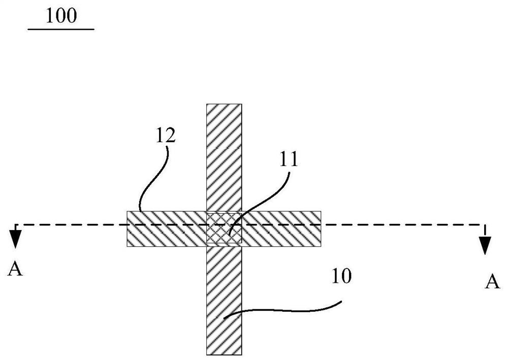
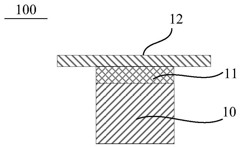
[0096]Still another embodiment of the present invention provides an electronic device, including a RRAM storage unit and electronic components connected to the RRAM storage unit. Wherein, the RRAM storage unit includes: a semiconductor substrate, an interlayer dielectric layer is formed on the semiconductor substrate, grooves are formed in the interlayer dielectric layer, and grooves are respectively located in the grooves. The first left electrode and the first right electrode on both sides; a resistive layer is formed on the side wall of the trench; a second electrode filling the trench is formed in the trench, wherein the The resistive layer between the first left electrode and the second electrode is the first resistive layer, the resistive layer between the first right electrode and the second electrode is the second resistive layer, and the first The resistance of the resistance variable layer changes based on the levels on the first left electrode and the second electro...
PUM
 Abstract
Description
Claims
Application Information
 - R&D
- Intellectual Property
- Life Sciences
- Materials
- Tech Scout
- Unparalleled Data Quality
- Higher Quality Content
- 60% Fewer Hallucinations
Browse by: Latest US Patents, China's latest patents, Technical Efficacy Thesaurus, Application Domain, Technology Topic, Popular Technical Reports.
© 2025 PatSnap. All rights reserved.Legal|Privacy policy|Modern Slavery Act Transparency Statement|Sitemap|About US| Contact US: help@patsnap.com