Supercharge Your Innovation With Domain-Expert AI Agents!

Epoxy molding compound for high power soic semiconductor packaging applications

An epoxy molding and compound technology, which is used in semiconductor devices, semiconductor/solid-state device components, electric solid-state devices, etc., and can solve problems such as being unsuitable for high-voltage applications.

Active Publication Date: 2021-10-29
HENKEL HUAWEI ELECTRONICS
View PDF7 Cites 0 Cited by
  • Summary
  • Abstract
  • Description
  • Claims
  • Application Information

AI Technical Summary

Problems solved by technology

However, they are not suitable for high pressure applications
[0006] To date, there has been no systematic study of epoxy molding compounds suitable for high-power SOIC semiconductor packaging applications

Method used


Image

  • Epoxy molding compound for high power soic semiconductor packaging applications
  • Epoxy molding compound for high power soic semiconductor packaging applications
  • Epoxy molding compound for high power soic semiconductor packaging applications

Examples


preparation example Construction

[0091] The method for preparing the epoxy molding compound of the invention is not particularly limited. In a preferred embodiment, the epoxy molding compound is prepared by a process comprising the following steps:

[0092] (1) Accurately weigh each component and mix it in a high-speed mixer for 20-30 minutes;

[0093] (2) Add liquid additives to the mixer and continue mixing for 15-20 minutes,

[0094] (3) Pass the mixed material through a twin-screw extruder, and knead the extruded material at 90-110°C,

[0095] (4) Finally the material is cooled and ground.

[0096] The epoxy molding compounds of the present invention are useful for packaging IC devices.

[0097] Epoxy molding compounds for IC devices can be cured by conventional molding methods such as transfer molding, compression molding, etc.
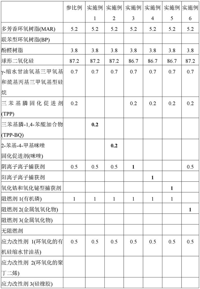
Embodiment 1

[0155] Polyaromatic epoxy resin (MAR), 5.2%

[0156] Phenol biphenyl aralkyl resin, 3.8%

[0157] Spherical silica, 87.2%

[0158] Gamma-glycidyloxytrimethoxy and mercaptopropyltrimethoxysilanes, 0.7%

[0159] Release agent, 0.6%

[0160] Epoxidized Silicone Glycidyl Resin Type Low Stress Modifier, 0.5%

[0161] Anion Ion Scavenger, 0.5%,

[0162] Organophosphorus flame retardant, 1%

[0163] Carbon pigment, 0.3%

[0164] Triphenylphosphine derivative, 0.2%

Embodiment 2

[0166] Polyaromatic epoxy resin (MAR), 5.2%

[0167] Phenol biphenyl aralkyl resin, 3.8%

[0168] Spherical silica, 87.2%

[0169] Gamma-glycidyloxytrimethoxy and mercaptopropyltrimethoxysilanes, 0.7%

[0170] Release agent, 0.6%

[0171] Epoxidized Silicone Glycidyl Resin Type Low Stress Modifier, 0.5%

[0172] Anion Ion Scavenger, 0.5%,

[0173] Organophosphorus flame retardant, 1%

[0174] Carbon pigment, 0.3%

[0175] 2-Phenyl-4-methylimidazole curing accelerator, 0.2%


PUM


Abstract

The invention relates to an epoxy molding compound, a preparation method and the use of the epoxy molding compound. The epoxy molding compound includes epoxy resin, phenolic resin, low stress modifier, ion trapping agent, curing accelerator and filler. Epoxy molding compounds can be used for high-power SOIC semiconductor packages with electrical leakage of less than 30μA at 180°C, while meeting JEDEC standards for reliability and lead-free reflow requirements at 260°C.

Description

technical field [0001] The invention relates to an epoxy molding compound, especially for high-power SOIC (Small Outline Integrated Circuit) semiconductor packaging applications, as well as a preparation method and application of the epoxy molding compound. Background technique [0002] Because epoxy resins have a good balance of properties including molding properties, electrical properties, moisture resistance, heat resistance, mechanical properties, and adhesion to components inserted into them, molded epoxy resin products are widely used in electrical and electronic Components of devices, such as transistors and integrated circuit boards. [0003] Molded epoxy products are prepared from epoxy molding compounds. Typical epoxy molding compounds comprise epoxy resins, curing agents (hardeners), curing accelerators (catalysts), and optionally fillers and additives. Epoxy molding compounds can be molded and cured into solid form articles by holding in a mold at elevated tem...

Claims


Application Information

Patent Timeline
Patent Type & Authority Patents(China)
IPC IPC(8): H01L23/29C08L63/00
CPCC08L63/00H01L23/293C08L61/04
Inventor 丁东金松陈波钱莹贾路方秦旺洋
Owner HENKEL HUAWEI ELECTRONICS
Features
  • R&D
  • Intellectual Property
  • Life Sciences
  • Materials
  • Tech Scout
  • Unparalleled Data Quality
  • Higher Quality Content
  • 60% Fewer Hallucinations
Learn More