Power semiconductor device and method for manufacturing power semiconductor device
A technology of semiconductor and electric power, which is applied in semiconductor/solid-state device manufacturing, semiconductor devices, semiconductor/solid-state device components, etc., can solve the problems of power module reliability loss and damage, and achieve the effect of high yield
- Summary
- Abstract
- Description
- Claims
- Application Information
AI Technical Summary
Problems solved by technology
Method used
Image

Examples
Embodiment approach 1
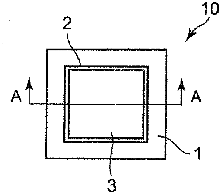
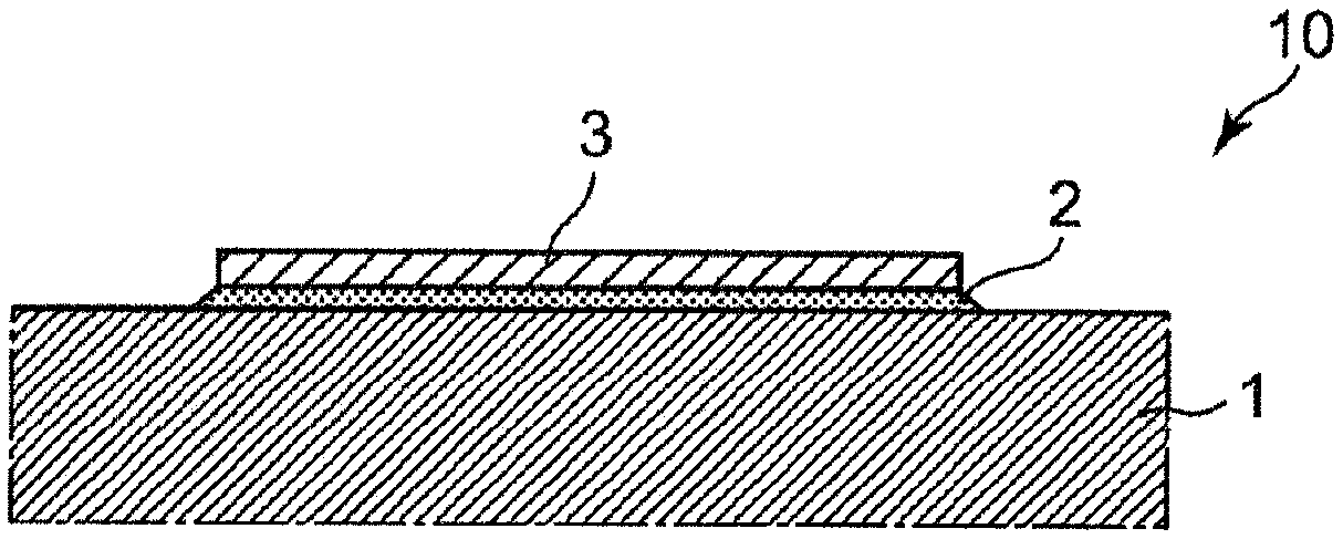
[0044] Figure 1A is a plan view showing power module 10 according to Embodiment 1 of the present invention, Figure 1B yes Figure 1A The A-A line profile. The power module 10 includes: a substrate 1; and a semiconductor element 3 bonded to the substrate 1 using a sinterable metal bonding material 2 (that is, provided via a bonding layer made of a sinterable metal bonding material).
[0045] The substrate 1 may also be a metal substrate such as copper (Cu) or aluminum (Al). In addition, the substrate 1 may be a ceramic substrate in which a conductive layer made of a metal such as Cu or Al is laminated and bonded to an insulating ceramic such as Al2O3, Si3N4, or AlN. Here, the conductive layer using this metal may be a single metal layer such as Cu or Al, or may be an example in which a noble metal material such as silver (Ag) or gold (Au) is coated on the metal layer. On the surface of the substrate 1 on which the semiconductor element 3 is mounted, a substrate electrode no...
Embodiment
[0068] Next, although Embodiment 1 of this invention is demonstrated concretely using an Example (samples S1-S4), these do not limit this invention. First, the substrate 1, the sinterable metal bonding material 2, and the semiconductor element 3 used in the examples will be described.
[0069] (Substrate 1)
[0070] A conductive layer using Cu, which is an example of a metal, is bonded to both surfaces of Si3N4, which is an example of an insulating ceramic, using brazing filler metal, to prepare a substrate 1 . The linear expansion coefficient of Si3N4 is about 3 ppm / °C, and that of Cu is about 17 ppm / °C. Therefore, the larger the thickness of the Cu plate, the larger the linear expansion coefficient of the substrate 1 as a whole. In order to reduce the stress applied to the semiconductor element 3 and the sinterable metal bonding material 2 and the resulting deformation, the Cu plate is preferably thin. Specifically, the thickness of the Cu plate is preferably 1.0 mm or le...
Embodiment approach 2
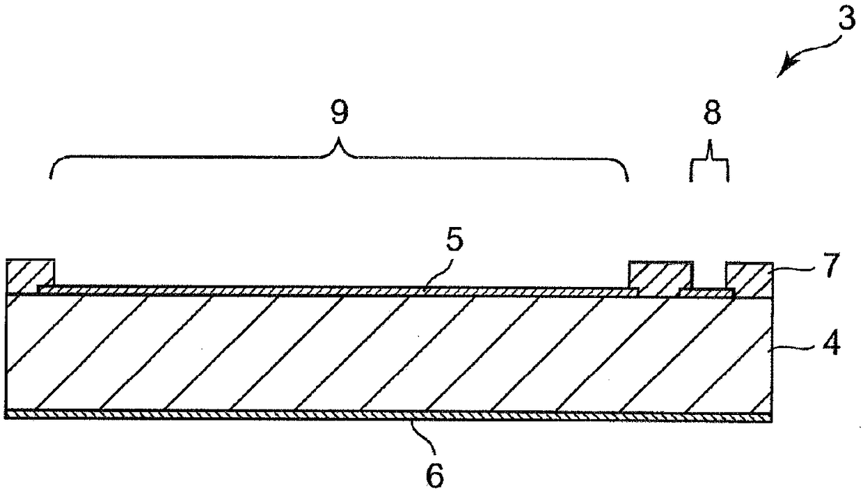
[0104] Figure 6 is the power module 20 according to Embodiment 2 of the present invention and Figure 1B Corresponding sectional view. Figure 7 yes Figure 6 Enlarged view of part of . In Embodiment 1, an example in which each of the surface metallization layer 5 and the backside metallization layer 6 of the semiconductor element 3 have a single-layer structure will be described. In Embodiment 2, an example in which the surface metallization layer 25 and the rear surface metallization layer 26 each have a multilayer structure will be described, and a preferable layer structure will be studied respectively. In addition, the power module 20 of the second embodiment has the same or corresponding components as the power module 10 of the first embodiment except for the layer structure of the surface metallization layer and the back metallization layer of the semiconductor element. In the description and drawings, the same reference numerals are assigned to these components, a...
PUM
 Abstract
Description
Claims
Application Information
 - R&D
- Intellectual Property
- Life Sciences
- Materials
- Tech Scout
- Unparalleled Data Quality
- Higher Quality Content
- 60% Fewer Hallucinations
Browse by: Latest US Patents, China's latest patents, Technical Efficacy Thesaurus, Application Domain, Technology Topic, Popular Technical Reports.
© 2025 PatSnap. All rights reserved.Legal|Privacy policy|Modern Slavery Act Transparency Statement|Sitemap|About US| Contact US: help@patsnap.com