Unlock instant, AI-driven research and patent intelligence for your innovation.

A kind of array substrate and display device

A technology for array substrates and display devices, which is applied to organic semiconductor devices, semiconductor devices, electrical components, etc., can solve the problems of complex process, high precision requirements, and great influence on luminous efficiency, and achieves a simplified process and reduced alignment accuracy. Effect

Active Publication Date: 2021-01-22
BOE TECH GRP CO LTD
View PDF5 Cites 0 Cited by
  • Summary
  • Abstract
  • Description
  • Claims
  • Application Information

AI Technical Summary

Problems solved by technology

[0003] In the prior art, in order to improve the transparency, a top emission structure is usually used to make a transparent display panel. Since the upper cover of the top emission is provided with structures such as a color filter and a black matrix corresponding to the pixel area of ​​the lower cover, the alignment deviation has a great influence on the luminous efficiency. Therefore, the top-emitting transparent display panel has high requirements for the alignment accuracy of the upper cover and the lower cover, and the process is relatively complicated.

Method used


Image

  • A kind of array substrate and display device
  • A kind of array substrate and display device
  • A kind of array substrate and display device

Examples


Embodiment Construction

[0040] In order to make the above objects, features and advantages of the present invention more comprehensible, the present invention will be further described in detail below in conjunction with the accompanying drawings and specific embodiments.

[0041] In the description of the present invention, unless otherwise stated, the meaning of "plurality" is two or more; the terms "upper", "lower", "left", "right", "inner", "outer" The orientation or positional relationship indicated by etc. is based on the orientation or positional relationship shown in the drawings, and is only for the convenience of describing the present invention and simplifying the description, rather than indicating or implying that the machine or element referred to must have a specific orientation, use a specific Azimuth configuration and operation, therefore, should not be construed as limiting the invention.

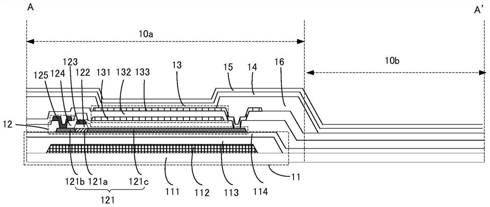
[0042] An embodiment of the present application provides an array substrate, referring to fi...


PUM


Abstract

The present application provides an array substrate and a display device, wherein the array substrate is a bottom-emitting OLED array substrate, including a plurality of pixel units, and each pixel unit is divided into a light-emitting area and a light-transmitting area, and the array of the light-emitting area The substrate includes: a substrate, and a driving transistor and a storage capacitor arranged on the substrate, and the display light passes through the storage capacitor and exits. The technical solution of the present application realizes transparent display through the OLED array substrate of the bottom emission structure. The light-emitting area is provided with a storage capacitor that can pass through the display light. Since it is a bottom emission structure, there is no need to set a black matrix on the packaging cover of the array substrate. Furthermore, the pixel units on the array substrate do not need to be precisely aligned with structures such as the black matrix on the package cover. Compared with the existing top-emitting structure to achieve transparent display technology, the array substrate provided by this application can reduce alignment accuracy and simplify craft.

Description

technical field [0001] The present invention relates to the field of display technology, in particular to an array substrate and a display device. Background technique [0002] With the development of the information society, novel display technologies such as transparent display devices have obtained good user experience and have broad market prospects. However, the transparent display panel and the transparent display device including the transparent display panel have not been commercialized so far because of the competition between the transparency of the transparent display device and the luminous efficiency of the panel. The design of enhancing the transparency of the transparent display panel will be at the expense of reducing the light-emitting area, thereby reducing the luminous efficiency, and vice versa. [0003] In the prior art, in order to improve the transparency, a top emission structure is usually used to make a transparent display panel. Since the upper co...

Claims


Application Information

Patent Timeline
Patent Type & Authority Patents(China)
IPC IPC(8): H01L27/32
CPCH10K59/1216H10K2102/3035
Inventor 王国英宋振
Owner BOE TECH GRP CO LTD