
A detection circuit and a liquid crystal display device
A technology for detecting circuits and display panels, used in measuring devices, static indicators, optical instrument testing, etc., can solve problems such as screen flicker, grayscale screen and solid-color screen flicker, inability to accurately detect the quality of display panels, and save borders. , the effect of suppressing flicker
- Summary
- Abstract
- Description
- Claims
- Application Information
AI Technical Summary
Problems solved by technology
Method used
Image

Examples
no. 1 example
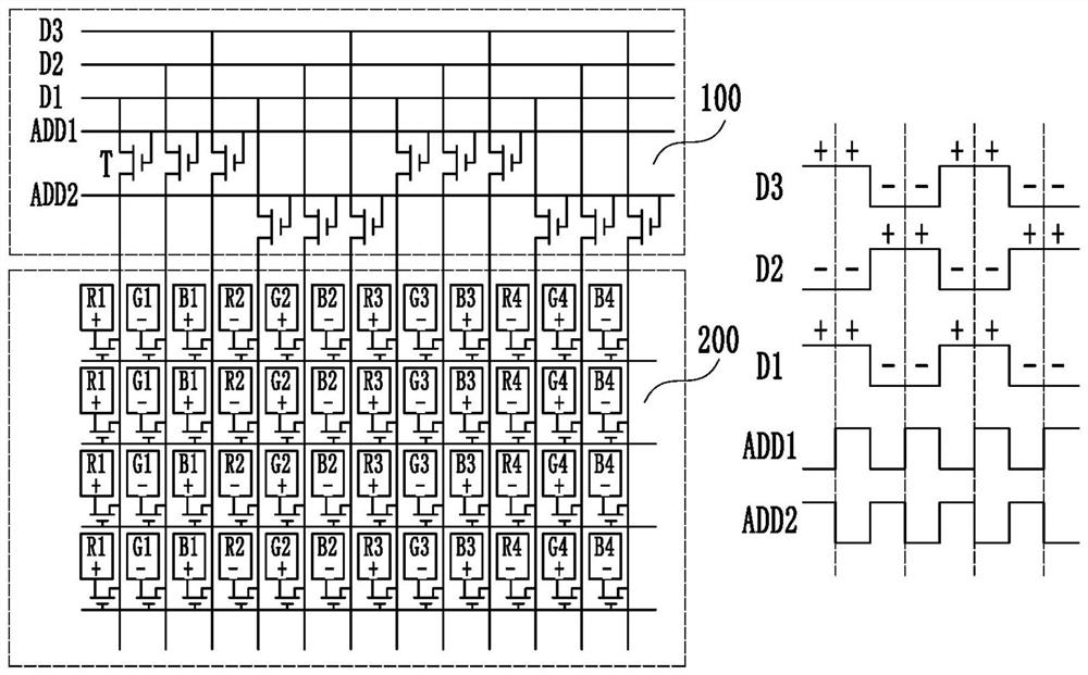
[0031] The detection circuit 100 of this embodiment is used to detect the display panel 200. The display panel 200 includes a plurality of pixel units arranged in an array, and each pixel unit includes three sub-pixels for displaying different colors, respectively the first sub-pixel (R1, R2, etc.), the second sub-pixel (G1, G2, etc.) and the third sub-pixel (B1, B2, etc.), the detection circuit 100 includes a plurality of switching elements T, at least two control signal lines and at least three data signals Wire.
[0032] Each of the multiple switching elements T includes a control terminal, a first channel terminal, and a second channel terminal. The first channel terminals of the multiple switching elements T are all connected to the same sub-pixel adjacent to each row along the column direction. The multiple switching elements T The control terminals of the plurality of switching elements T are all connected to a corresponding one of the at least two control signal lines,...
no. 2 example
[0045] R0, R1, R2, R3, R4, etc. in the drawings of this specification represent each first sub-pixel, G0, G1, G2, G3, G4, etc. represent each second sub-pixel, B0, B1, B2, B3, B4, etc. denote the respective third sub-pixels. Please refer to image 3 , image 3 It is a detection circuit 100 and a waveform diagram of an embodiment. image 3 In the detection circuit shown, the first channel ends of the plurality of switch elements (T) are connected to the upper and lower corresponding sub-pixels of any two adjacent rows. Now, the six sub-pixels of two adjacent pixel units in each row are the first sub-pixel R1, the second sub-pixel G1, the third sub-pixel B1, the fourth sub-pixel R2, the fifth sub-pixel G2 and the sixth sub-pixel The sub-pixel B2 is taken as an example for description.
[0046] The structure of the detection circuit 100 of this embodiment is basically the same as that of the detection circuit 100 of the first embodiment, the only difference is that the detect...
no. 3 example
[0054] Please refer to Figure 5 , Figure 5 It is a detection circuit 100 and a waveform diagram of an embodiment. The structure of the detection circuit 100 of this embodiment is basically the same as that of the detection circuit 100 of the second embodiment. Pixels are connected.
[0055] Specifically, in the first time period of the first frame, the control signal on the first control signal line ADD1 is at a high level, and the corresponding three switching elements T are turned on, so that the six sub-pixels of any adjacent two groups of pixel units Three of the sub-pixels are respectively connected to the three data signal lines one by one and obtain corresponding polarities. For example, an embodiment such as Figure 5 As shown, in the first time period of the first frame, the control signal on the first control signal line ADD1 is at a high level, and the corresponding three switching elements T are turned on, so that the six sub-pixels of any adjacent two groups...
PUM
 Abstract
Description
Claims
Application Information