
Magnetic analyzer unit

A magnetic analyzer and magnetic field technology, applied in electrical components, discharge tubes, circuits, etc., can solve problems affecting the electrical properties of doped semiconductor materials and reducing the ion purity of semiconductor materials

Inactive Publication Date: 2019-02-01
HUAIAN IMAGING DEVICE MFGR CORP
View PDF3 Cites 0 Cited by
  • Summary
  • Abstract
  • Description
  • Claims
  • Application Information

AI Technical Summary

Problems solved by technology

However, existing magnetic analyzer cell designs are limited in blocking unwanted impurity particles, which may reduce the purity of the ions implanted into the semiconductor material, thereby affecting the electrical properties of the resulting doped semiconductor material

Method used


Image

  • Magnetic analyzer unit
  • Magnetic analyzer unit
  • Magnetic analyzer unit

Examples


example 1

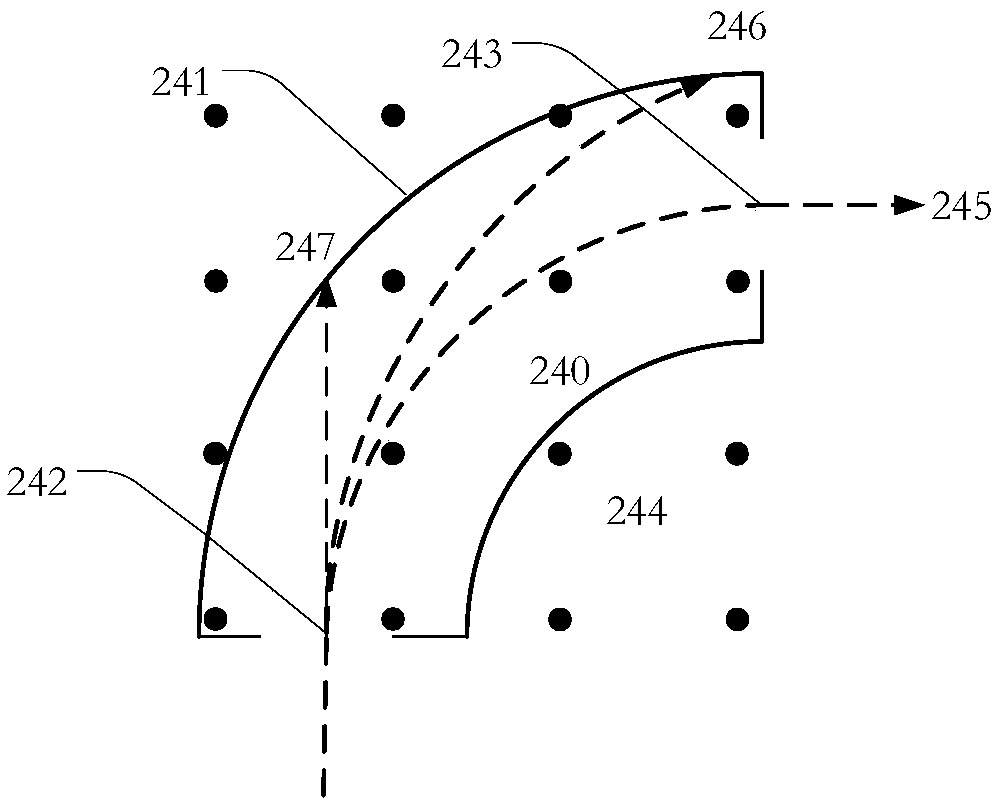
[0072] Example 1. A magnetic analyzer unit comprising:

[0073] a receiving end opening configured to receive the flow of ions from the ion source;

[0074] an output opening configured to output ions having a particular mass-to-charge ratio in the ion stream;

[0075] an ion channel connecting the receiving end opening and the output end opening, and the ion channel includes at least one U-shaped channel segment;

[0076] Wherein, the at least one U-shaped channel section is arranged in a magnetic field configured to enable the ions having a specific mass-to-charge ratio to pass through the at least one U-shaped channel section.

example 2

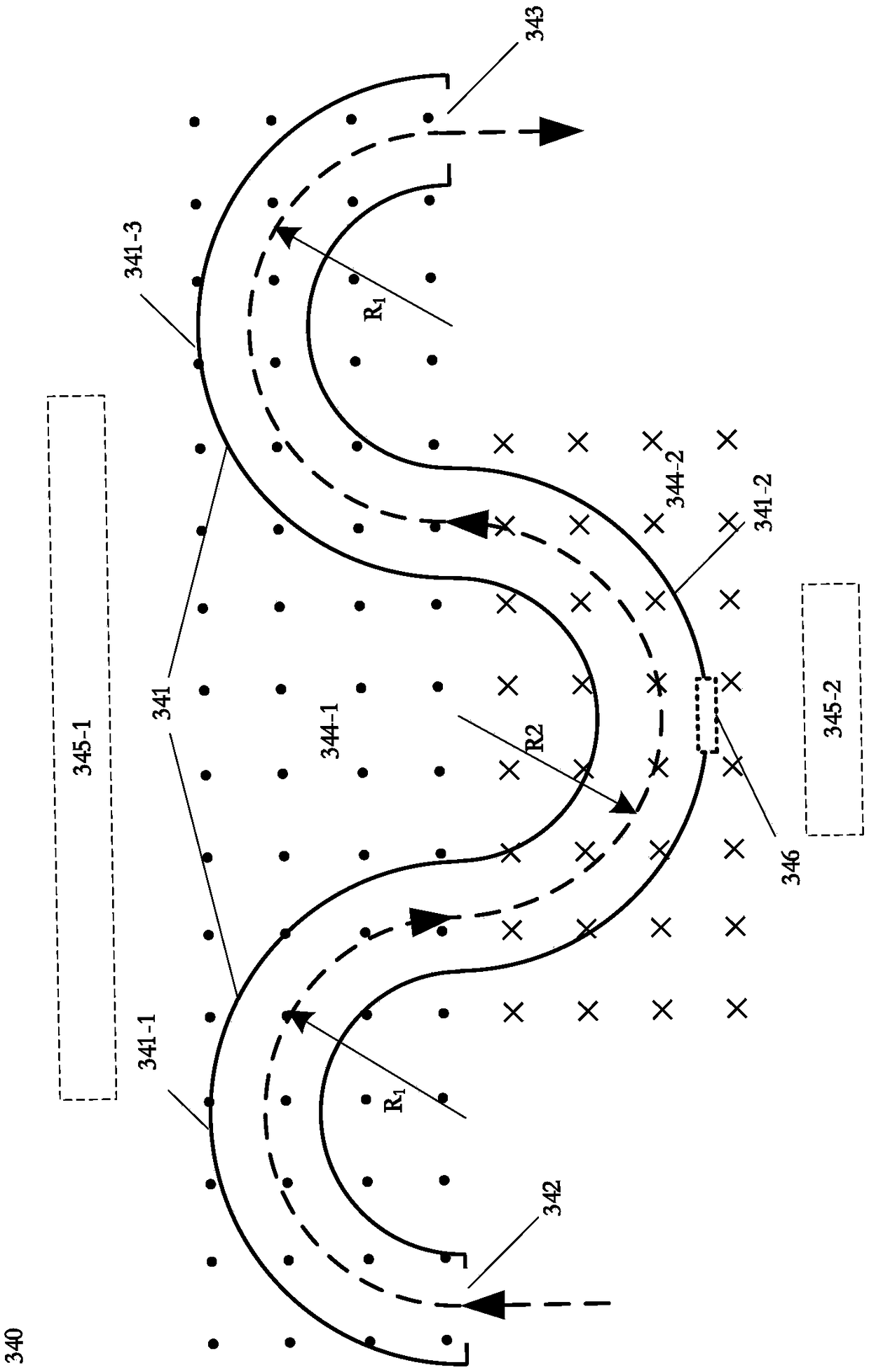
[0077] Example 2. The magnetic analyzer unit of example 1, wherein:

[0078] The magnetic field includes at least a first magnetic field configured to cause the ions having a specific mass-to-charge ratio to rotate in a first rotation direction, and a second magnetic field configured to have a specific mass-to-charge ratio. The charged ions are rotated in a second direction of rotation, the second direction of rotation being different from the first direction of rotation.

example 3

[0079] Example 3. The magnetic analyzer unit of example 2, wherein:

[0080] The at least one U-shaped channel section comprises a cascaded plurality of U-shaped channel sections.


PUM


Abstract

The present invention relates to a magnetic analyzer unit. The magnetic analyzer unit comprises a receiving end opening, an output end opening and an ion channel; the receiving end opening is configured to receive ion current from an ion source; the output end opening is configured to output ions having a specific mass-to-charge ratio in the ion current; the ion channel is connected with the receiving end opening to the output end opening; and the ion channel comprises at least one U-shaped channel section, wherein the at least one U-shaped channel section is disposed in a magnetic field, wherein the magnetic field is configured to enable the ions having the specific mass-to-charge ratio to pass through the at least one U-shaped channel section.

Description

technical field [0001] The present disclosure relates to the field of semiconductors, and in particular, to a magnetic analyzer unit. Background technique [0002] In the production process of semiconductor devices, in order to enable semiconductor materials to exhibit specific electrical characteristics (such as forming a PN junction), it is often necessary to dope a certain type of ion into the semiconductor material according to a certain concentration and distribution to change Electrical properties of semiconductor materials. Ion implantation is a common doping method. Some ion implantation processes involve accelerating a specific type of ions generated by an ion source toward the surface of a semiconductor material (eg, silicon material), thereby enabling the specific type of ions to enter the semiconductor material. However, impurity particles other than the desired specific type of ions inevitably exist in a system for ion implantation. In order to ensure ideal e...

Claims


Application Information

Patent Timeline
IPC IPC(8): H01J37/05H01J37/317
CPCH01J37/05H01J37/317H01J2237/055H01J2237/31705
Inventor 杨健李天慧黄晓橹
Owner HUAIAN IMAGING DEVICE MFGR CORP
Features
  • Generate Ideas
  • Intellectual Property
  • Life Sciences
  • Materials
  • Tech Scout
  • Unparalleled Data Quality
  • Higher Quality Content
  • 60% Fewer Hallucinations
Learn More