Check patentability & draft patents in minutes with Patsnap Eureka AI!

OLED device and method of making the same

A manufacturing method and packaging structure technology, applied in the direction of organic semiconductor devices, semiconductor devices, electrical components, etc., can solve the problem that the packaging structure of the OLED bending area is prone to cracks, etc., and achieve the effect of not being easily broken

Active Publication Date: 2021-06-25
WUHAN CHINA STAR OPTOELECTRONICS SEMICON DISPLAY TECH CO LTD
View PDF5 Cites 0 Cited by
  • Summary
  • Abstract
  • Description
  • Claims
  • Application Information

AI Technical Summary

Problems solved by technology

[0004] The invention provides an OLED device and a manufacturing method thereof, so as to solve the technical problem that the packaging structure of the OLED bending area is prone to cracks in the prior art

Method used


Image

  • OLED device and method of making the same
  • OLED device and method of making the same
  • OLED device and method of making the same

Examples


Embodiment Construction

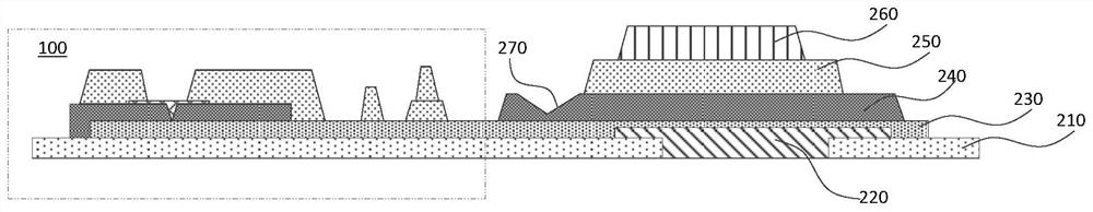
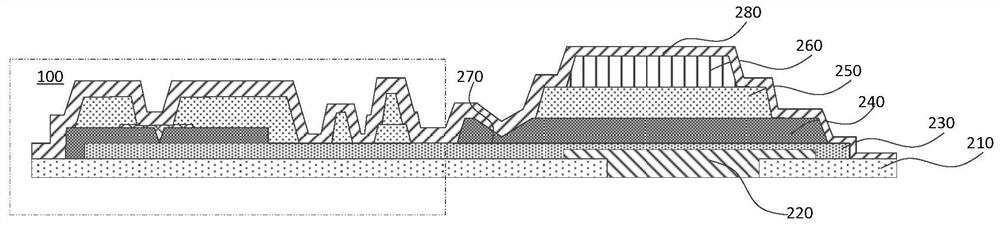
[0027] The following descriptions of the various embodiments refer to the accompanying drawings to illustrate specific embodiments in which the invention may be practiced. The directional terms mentioned in the present invention, such as [top], [bottom], [front], [back], [left], [right], [inside], [outside], [side], etc., are only for reference The orientation of the attached schema. Therefore, the directional terms used are used to illustrate and understand the present invention, but not to limit the present invention. In the figures, structurally similar elements are denoted by the same reference numerals.

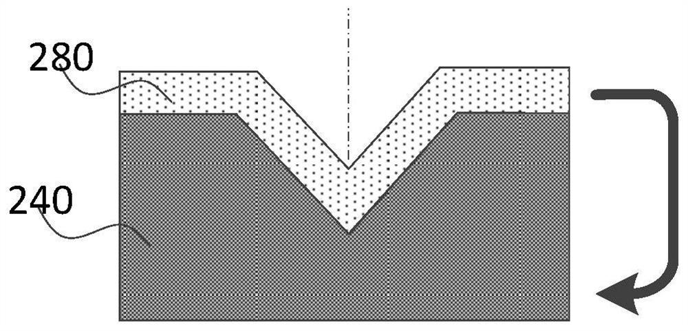
[0028] The invention provides an OLED device and a manufacturing method thereof to solve the technical problem in the prior art that the packaging structure of the OLED bending area is prone to cracks.

[0029] Specifically, see figure 1 , the present invention provides an OLED device, which includes a substrate 210, a display area 100 located on the first surface of ...


PUM


Abstract

The invention provides an OLED device and a manufacturing method thereof. The OLED device shown includes a substrate, a display area on the first surface of the substrate, a non-display area on both sides of the display area, and an encapsulation structure covering the display area and the non-display area; wherein, the non-display area The display area is composed of a bendable flexible substrate, the flexible substrate is bent towards the second surface of the substrate, the second surface is opposite to the first surface, and is located on the back of the first surface; the non-display area and At least one groove structure is provided at an adjacent edge of the display area, and the groove structure extends along a first direction, and the first direction is a direction parallel to the boundary line between the display area and the non-display area ; The encapsulation structure includes an inorganic thin film covering the display area, the non-display area and the groove structure. The invention can solve the technical problem that the packaging structure of the OLED bending area is prone to cracks in the prior art.

Description

technical field [0001] The invention relates to the field of electronic display, in particular to an OLED device and a manufacturing method thereof. Background technique [0002] In order to further increase the screen-to-body ratio of the OLED display, that is, the ratio of the area of ​​the display area to the area of ​​the display, those skilled in the art have proposed a flexible frame, that is, digging holes in the non-display area of ​​the display, and then Metal wiring layout and organic layer coating, and then the non-display area is bent downward, thereby reducing the projected area of ​​the non-display area on the display screen, thereby increasing the screen-to-body ratio. [0003] Typically, the organic layer in the bend region is exposed to the atmosphere and its surface is not encapsulated. This is because the inorganic thin film used for encapsulation has poor ductility and is prone to cracks when bent. If the cracks spread to the display area, the screen wil...

Claims


Application Information

Patent Timeline
Patent Type & Authority Patents(China)
IPC IPC(8): H01L27/32H10K99/00
CPCH10K59/124H10K59/1213H10K71/00H10K59/873Y02E10/549H10K59/131H10K77/111H10K2102/311H10K50/844
Inventor 张兴永
Owner WUHAN CHINA STAR OPTOELECTRONICS SEMICON DISPLAY TECH CO LTD
Features
  • R&D
  • Intellectual Property
  • Life Sciences
  • Materials
  • Tech Scout
  • Unparalleled Data Quality
  • Higher Quality Content
  • 60% Fewer Hallucinations
Learn More